
Printed and flexible electronics
The main drive for our activities is to bridge a gap between the nano-world and real life applications. In particular, solution processable semiconducting nano-blocks, including inorganic nanowires, conjugated polymers and carbon nanotubes can be deposited by wet-coating methods and various self-assembly techniques to result in large area electronics.
Overview
Solution-based fabrication of electronic and opto-electronic devices using functional ‘inks’ at low temperatures and on large area substrates is an attractive printed electronics technology for the development of low-cost, lightweight and flexible electronics, including:
- Circuits
- Displays
- Energy harvesting and storage devices
- Lasers
- Memory elements
- Reconfigurable antennas
- Sensors.
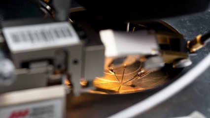
We utilise a variety of printing techniques for materials deposition including ink-jet printing, screen printing, slot-die coating, wire bar coater to produce the most important electronics ‘building blocks’ such as field-effect transistors, diodes, photovoltaic cells, photoconducting elements, photodiodes and sensors. Fabrication of conducting tracks is essential for all types of devices.
The ability to produce customisable, digitally printable, antennas and reflectors for RF applications with integrated printable switching elements has opened vast opportunities for low-cost fabrication of microwave devices.
What we print
- Dielectrics (polymers, spin-on-glass).
Semiconducting materials
- Organic semiconductors (polymers and small molecules)
- Nanomaterials (semiconducting nanowires, CNTs).
Conductors
- Metal nanoparticles
- Conducting polymers (PEDOT:PSS)
- Composites (PEDOT:PSS and carbon nanotubes).
Research areas
Polymer field-effect transistors (FETs) are promising candidates for the fabrication of low-cost electronic circuits and pixel drivers, due to the potential of depositing all device elements from solution into layered thin-film structures and onto flexible substrates.
References
S. Georgakopoulos, D. Sparrowe, F. Meyer, M. Shkunov, “Stability of top- and bottom-gate amorphous polymer field-effect transistors”, Appl. Phys. Lett. 97, 243507, 2010.
To fully realise the promise of flexible, ink-jet-printed electronics for radio frequency and microwave applications, there is a need for robust metrology to characterise the inks and the circuits that are fabricated.
In our laboratories and with our partners we have the capability of performing high-accuracy, with uncertainties, of calibrated measurements of inkjet printed circuits. Here at the University of Surrey this is supported in our new nonlinear microwave measurement and modelling laboratory, which is backed by a £2M Strategic Equipment Grant from EPSRC.
Partner institutes
- National Physical Laboratories, Teddington, UK
- Department of Electrical Engineering and Computer Science, The University of Toledo, USA
- Institute of Electronic Systems, Warsaw University of Technology, Warsaw, Poland
- National Institute of Standards and Technology Boulder, Colorado, USA.
Publications
A. Sahu, V. Devabhaktuni, A. Lewandowski, P. Barmuta, T. M. Wallis, M. Shkunov, and P. H. Aaen, “Microwave Characterization of Ink-Jet Printed CPW on PET Substrates”, accepted for publication at the 86th ARFTG Microwave Measurement Conference, 1 - 4 December, 2015.
The Source-Gated Transistor (SGT) is a type of electronic device invented at the University of Surrey.
Due to its mode of operation, the SGT has several advantages over conventional transistors, particularly in low-power, mixed-signal (analogue/digital) applications which are very cost-sensitive. We are investigating the implementation of the SGT using new materials and fabrication techniques such as inkjet printing, which would enable large-area electronic circuits to be realised with improved performance, lower energy demands and reduced cost.
References
E Bestelink, U Zschieschang, I Bandara RM, H Klauk, RA Sporea, “The Secret Ingredient for Exceptional Contact‐Controlled Transistors”, Advanced Electronic Materials 8 (4), 2101101, 2021.
Radu A. Sporea Kham M. Niang Andrew J. Flewitt S. Ravi P. Silva, "Novel Tunnel‐Contact‐Controlled IGZO Thin‐Film Transistors with High Tolerance to Geometrical Variability", Advanced Materials, 31 (36), 1902551, 2019.
R. A. Sporea, M. J. Trainor, N. D. Young, J. M. Shannon, S. R. P. Silva, “Intrinsic Gain in Self-Aligned Polysilicon Source-Gated Transistors”, IEEE Trans. Electron. Devices, vol. 57, iss. 10, 2010.
Future large area electronic systems such as wearable, fully printed, and flexible applications require innovations in materials, device design and fabrication processes.
Dr Radu Sporea held the prestigious Royal Academy of Engineering Academic Research Fellowship (2011-2016). The project covered several aspects of future large-area electronic device and circuit design, including:
- New transistor architectures for improved energy efficiency
- Strategies for reducing performance variations due to processing variability
- Reliability improvements for thin-film transistors
- Sub-micron super-resolution printing of electrode gaps for transistors and sensors
- Exploitation of material properties for optimal device operation, e.g. field-dependent mobility
- Modelling of device-circuit interaction, contact effects and fundamental behaviour of semiconductor devices
- Circuit block design optimised for application.
- Compact modelling and development of design toolkit for unipolar logic circuits
Collaborations
- Shanghai Jiao Tong University, China
- University of Tours, France
- Cambridge University, U.K.
Selected publications
Dahiya A. S, Sporea Radu, Poulin-Vittrant G., Alquier D. (2019) Stability evaluation of ZnO nanosheet based source-gated transistors, Scientific Reports 9 (1).
R. A. Sporea, T. Burridge & S. R. P. Silva “Self-Heating Effects In Polysilicon Source Gated Transistors”, Scientific Reports 5,14058 (2015).
Q Cui, RA Sporea, W Liu, X Guo, “Analytical Models for Delay and Power Analysis of Zero-Load Unipolar Thin-Film Transistor Logic Circuits”, Electron Devices, IEEE Transactions on, 61 (11), 3838 - 3844 (2014).
R. A. Sporea, M. J. Trainor, N. D. Young, J. M. Shannon & S. R. P. Silva, “Source-gated transistors for order-of-magnitude performance improvements in thin-film digital circuits”, Scientific Reports 4, 4295 (2014).
Sporea, R.A.; Alshammari, A.S. ; Georgakopoulos, S. ; Underwood, J. ; Shkunov, M. ; Silva, S.R.P. , “Micron-scale inkjet-assisted digital lithography for large-area flexible electronics”, Solid-State Device Research Conference (ESSDERC), 2013 Proceedings of the European, 280 – 283, (2013).
Shannon, J.M.; Sporea, R.A.; Georgakopoulos, S.; Shkunov, M.; Silva, S.R.P., "Low-Field Behavior of Source-Gated Transistors," in Electron Devices, IEEE Transactions on , vol.60, no.8, pp.2444-2449, Aug. 2013.
Opoku, C., Chen, L., Meyer, F. & Shkunov, M. “Solution Processable Nanowire Field-Effect Transistors”. MRS Online Proceedings Library 1287, (2011).
X. Guo et al., "High Performance Transistors in Low Mobility Organic Semiconductors for Analog and High-Frequency Applications," in Flexible Electronics and Displays Conference and Exhibition, 2008 , vol., no., pp.1-5, 21-24 Jan. 2008.
Assembly of field-effect transistors (FETs) using semiconducting inks at low temperatures on large areas, and on optically transparent substrates, are finding potential applications in many areas including: Sensors, RFID tags, memory elements, and flexible display applications.
Single-crystalline semiconducting nanowires are offering potential breakthroughs in the area of high performance, low cost device assembly due to their proven high charge carrier mobility and compatibility with solution based assembly. Their unique aspect ratio permits nanowires to be dispersed in solvents and processed as inks to ‘bridge’ device electrodes at room temperature.
References
C. Opoku, L. Chen, F. Meyer, M. Shkunov “Solution Processable Nanowire Field-Effect Transistors”, MRS Proceedings, 1287, 2011, mrsf10-1287-f10-03 doi:10.1557/opl.2011.1437.
Projects
- EPSRC “From nanowires to printed electronics”, (EP/I017569/1)
- EU: “HOMES”, Indoor communication terminal with flexible Substrate, European programme INTERREG IVA 2007-2013 France (Channel) – England, Ref. 5700/4289 & FEDER Upper-Normandy Region
- Industry funded: “Nanowire field-effect transistors for sensor applications”
- NPL funded: “Advanced characterisation of semiconducting materials for electronic devices.”
Academic and industrial collaborations
- National Physical Laboratory, Teddington, UK
- The University of Texas, Austin, Department of Chemical Engineering, USA
- National Institute of Standards and Technology, Boulder (Colorado) and Gaithersburg (Maryland), USA
- Australian National University, Department of Electronic Materials Engineering, Canberra, Australia
- More than 10 UK based companies
- University of Kent, School of Engineering and Digital Arts, Kent , UK
- ESIGELEC/IRSEEM, Rouen, France.