Future technologies for electrical isolation of III-V Semiconductor devices
Overview
Ion implantation is a well-proven technique for the selective creation of high-resistivity regions in compound semiconductors. Known as implant isolation, it is widely used to obtain inter-device electrical isolation with the significant advantage over selective wet or dry etching of maintaining the planarity of the wafer surface.
There are two different mechanisms for the production of implant-isolated regions in III-V semiconductors. In both cases compensation results from the trapping of carriers by the deep-level centres which are not thermally ionised at normal device operating temperatures.
The first relies on the implantation of a species which either by itself or in combination with impurities or dopants already present in the material, creates a chemically active deep-level state (e.g. O, Fe, Cr). The second method, and that which is more commonly used, requires ion bombardment of neutral species like B+, He+, or H+ to create damage-related deep levels in the material.
In this latter case, the isolation results from the induced lattice damage and hence it is dependent on a variety of parameters such as ion mass, dose, energy, and substrate temperature during implantation. Post-implantation annealing is usually required to maximise the resistivity.
This project was funded for three years by the EPSRC. It was a collaboration by researchers at the University of Surrey, University of Manchester Institute of Science and Technology (UMIST) and University College London (UCL).
Aims and objectives
The goals of the project were threefold:
- To gain a detailed physical understanding of the electrical isolation of III-V semiconductor materials using ion implantation and to use the data obtained from these fundamental measurements.
- Optimise present techniques used for isolation.
- Develop technology to enable implant isolation to be expanded to the fabrication of devices for which no reliable method currently exists.
In order to demonstrate the effectiveness of the isolation techniques developed, we intend to use implantation in the fabrication of devices such as HBTs and MQW Saturable Absorbers for which no satisfactory implant isolation procedure currently exist. Thus fabrication of planar devices can be successfully achieved.
Outputs
GaAs based materials
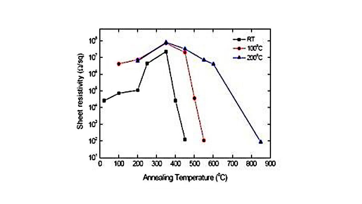
The first important experiment was to carry out implants into GaAs substrates held at temperatures above room temperature. We found that such elevated temperature (200oC) implants of protons provided much better thermal stability [1.] and in general a wider process window (figure 1); the technique is now being used in production.
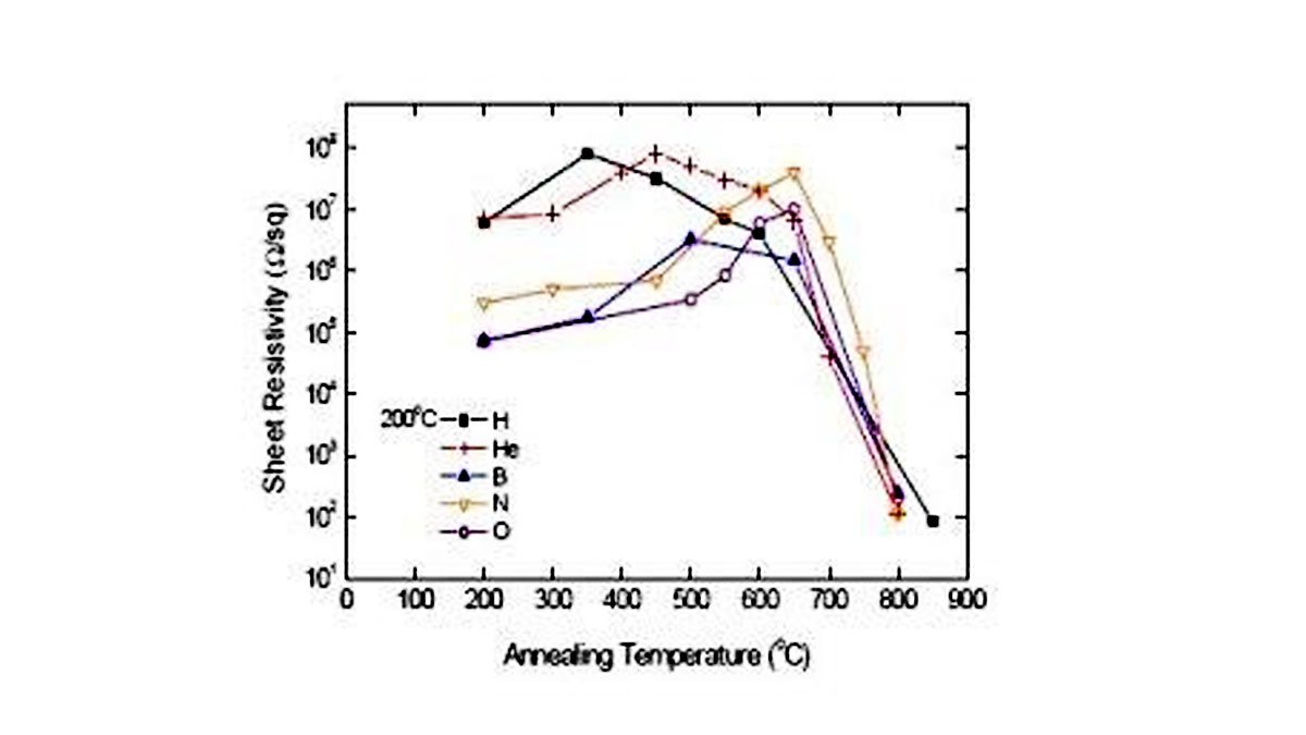
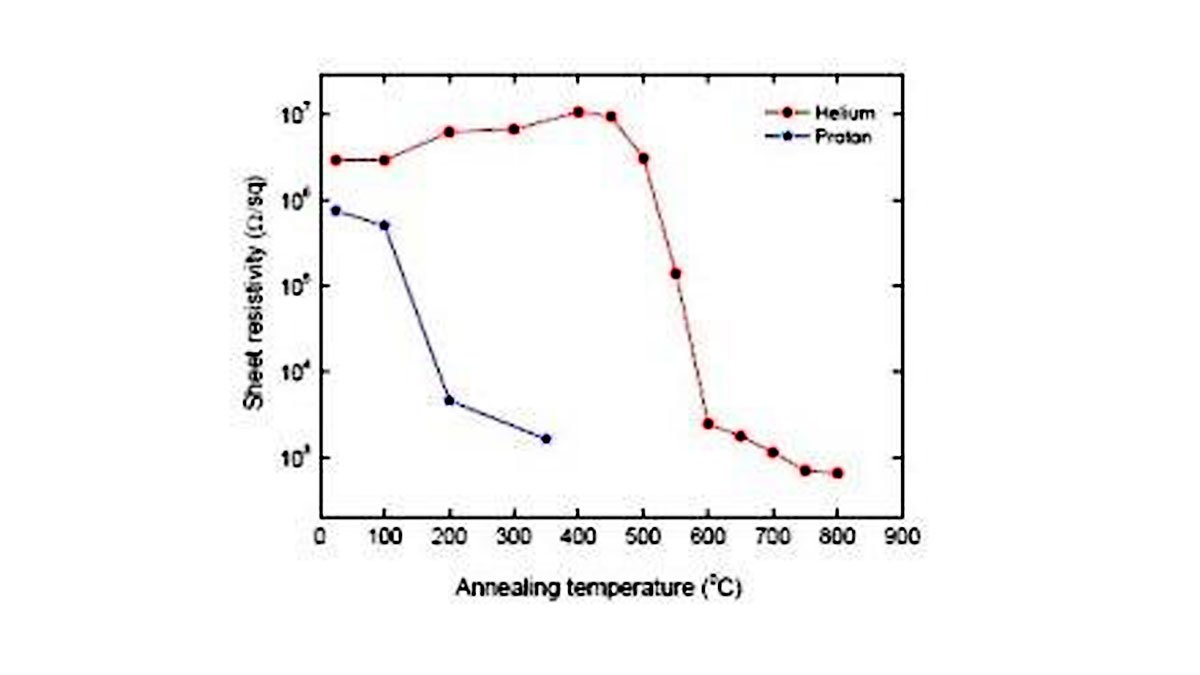
The use of helium ions was found to produce even higher sheet resistances and an improved thermal stability (process window of 200oC– 650oC), when implants were performed hot rather than at lower temperatures (figure 2) [2.]. Unlike protons and helium ions, boron, nitrogen and oxygen ions [3.] produced only a small effect on the sheet resistance as the implant temperature was changed.
For all these ion species, the optimum annealing temperature to obtain maximum sheet resistance was found to increase with increasing ion mass and was a maximum of about 650oC in the case of oxygen compared with a value of 350oC for protons (figure 2) [3.].
We also developed the use of threshold dose, which is the minimum dose to produce a maximum resistance for a given ion species and given implant conditions. We found that subsequent annealing of material implanted with protons at room temperature to the threshold dose produced the best material with sheet resistances of 108ohms/square.
We have investigated the effects of a range of ion species (H, He, B, N, O) implanted into GaAs at substrate temperatures of 77K, RT, 100oC, 200oC, doses between 1013 cm-2 and 1015 cm-2 and ion energies up to several MeV.
Whilst any of these ions can produce high resistance material, which ion is preferred depends on the material to be isolated. For example, if very thick layers need to be isolated then only protons may be used, because only they have sufficient penetration depth, and by choice of implant and annealing conditions, the maximum resistance can be achieved. We have developed an empirical relationship between the implant conditions, which dictate the amount of damage introduced and ultimately the resistance produced. Included in this relationship is the ion dose and the ion species.
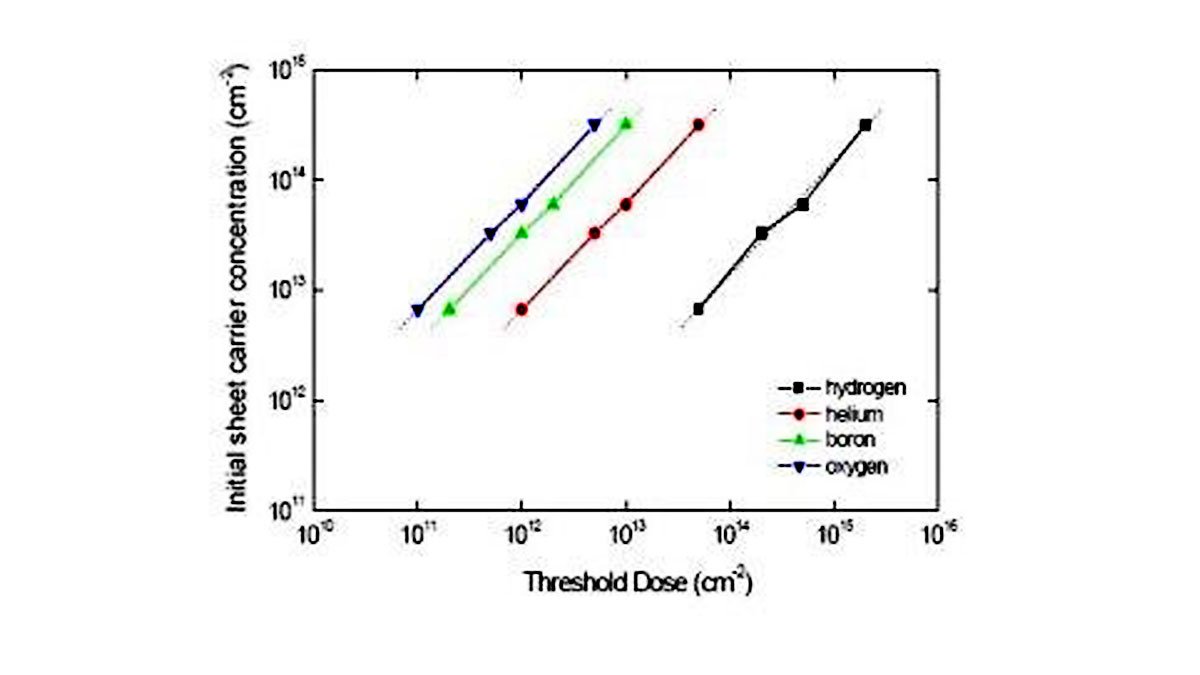
We found that for each ion species, (H, He, B, O) the initial carrier concentration is linearly dependent on the threshold dose (figure 3) and that for a given initial carrier concentration the damage introduced decreases linearly with threshold dose for each ion mass [4.]. Here the damage (energy deposited) is calculated using our simulation code SUSPRE which, knowing the initial carrier concentration and thickness of the conducting material and a material dependent carrier removal efficiency parameter, can be used to determine the threshold dose.
Using the more conventional SRIM Monte Carlo programme takes many minutes whereas SUSPRE takes just a few seconds to determine a threshold dose value. We have shown that the same analysis can be applied to other materials such as GaAsN, GaN and ZnO.
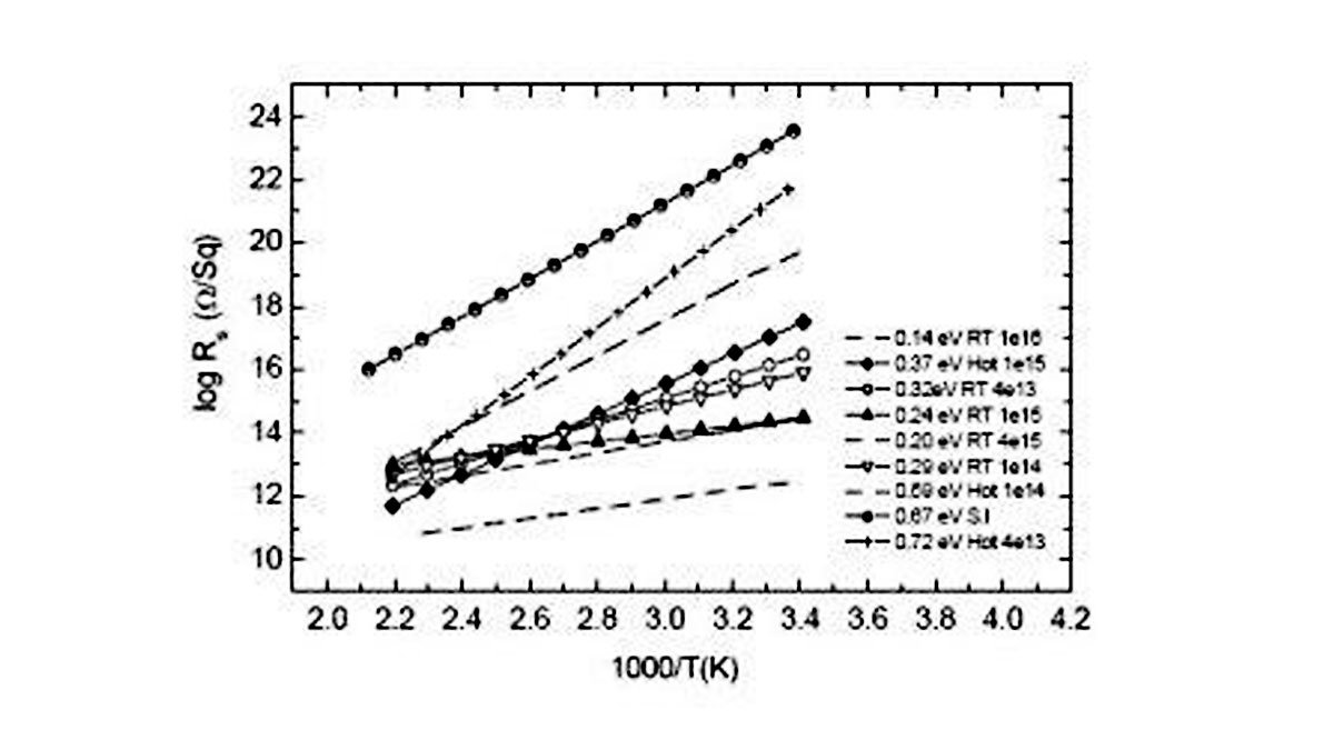
One of the most informative sets of data concerning defects were the plots of sheet resistance versus reciprocal temperature, which produced a series of up to nine activation energies ranging from 0.14eV to 0.7eV (figure 4). The activation energy corresponds to the major defect responsible for conduction in each sample.
We note that as the dose increases the activation energy decreases, so for large concentrations it is the shallow defects (0.14eV) which dominate the conduction process. On annealing such samples, the activation energy increases to values of 0.6, 0.67 and 0.71eV corresponding to high sheet resistance values. Thus the shallow defects need to be removed and the deeper defects need to form in order to obtain a maximum sheet resistance.
In a similar way, as the implant temperature is increased, deeper defects form, which explains why hot implants are more thermally stable than room temperature implants. The equivalent activation energy for bulk semi-insulating GaAs was measured to be 0.72eV, which corresponds to the well known EL2 defect.
InP based materials
Early work showed that protons could be used to isolate p-type InP in a similar way to GaAs, but ntype InP posed some difficulty and the sheet resistance attained was low allegedly due to the Fermi level being pinned in the top half of the bandgap.
More recent work has reported somewhat higher values of sheet resistance, so there is some uncertainty as to what value of sheet resistance can be achieved in n-type and p-type InP. A major problem is the poor thermal stability when using protons, but we found that using helium ions gives a great improvement up to about 500oC (figure 5).
We determined the sheet resistance as a function of temperature for helium implants and found that at least four activation energies could be identified between 0.23eV and 0.55eV, with the lowest only present for room temperature implants [5.]. High and thermally stable sheet resistances have been found for helium in n-type InP (figure 3), but similar treatment of InGaAs produces sheet resistances a factor of 100 lower. Proton implants produce even lower resistances in both n-type InP and n-type InGaAs [6.].
One of the major aims of this work was to develop a process for electrical isolation of both these materials and so we looked at ways of improving the poor results obtained for both protons and helium ions. Thus, we implanted iron ions which have been shown to be promising by other authors, although there is still little in the literature on the use of such implants. We produced sheet resistances of about 107 ohms/square in both n-type and p-type InP which were stable up to at least 500oC, with the p-type material having slightly higher resistance [7.8.].
Unlike GaAs there was no advantage in implanting InP above room temperature which seems to be connected with the position of the majority defect within the bandgap. It suggests that if shallower defects are formed in InP they are annealed out during the implantation process.
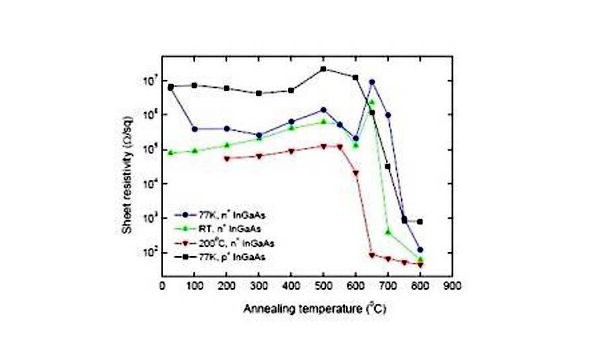
Iron was also implanted into InGaAs and produced sheet resistances of almost 106 ohms/square, with slightly higher values being recorded for 77K implants compared with those obtained at room temperature. These layers were stable up to about 500oC.
However, a second higher resistance peak was observed at about 650oC (identical results were obtained for InP) (figure 6). Implants into p-type InGaAs produced even higher resistance values, about 107 ohms/square, with a maximum of 2x10⁷ ohms/square occurring after annealing at 500oC, but it was necessary to implant at 77K to get this very high value (figure 6) [8.]. Iron implanted InGaAs layers were stable up to about 600oC.
In order to explain the presence of the second peak at about 650oC, we also implanted krypton ions under similar conditions to the iron implants in InP. Here we found that the sheet resistance followed the same trend as for iron implants but there was no second peak in resistance at 650oC, which suggests that this peak is associated with the presence of the iron.
We argue that in accord with published data, the peak at 650oC is due to the production of complex defects of iron and neighbouring vacancies (FeV). The carrier removal at temperatures up to 500oC is due solely to the damage introduced by the implant and not to the presence of iron. Iron atomic profiles show that it does not diffuse below 600oC and that even after higher temperature anneals, the material remains conducting even though much iron remains within the structure.
Usually In-based devices are made of several layers of different materials such as InP, InGaAs and InGaAsP. So we also studied carrier removal in the quaternary material, choosing nitrogen ions since we also used this ion species to create trapping centres for the fabrication of MQW saturable absorbers for our collaborators at UCL.
We compared the effects of 4MeV nitrogen implants into n-type InP and n-type InGaAsP and found that the sheet resistance did not saturate for the quaternary up to a dose of 1014 cm-2, whereas in the case of InP the threshold dose was found to be about 5x1013 cm-2.
For the InGaAsP, the sheet resistance increased with increasing dose up to a value of 1014 N+cm-2 and was identical for both 77K and room temperature implants. The maximum sheet resistance was below 105ohms/square which is lower than the few values reported in the literature. Thus it would appear that we did not implant a sufficiently high dose to get the highest possible sheet resistance.
This experiment was the last done in the project and unfortunately it did not produce a process to obtain the highest resistances in GaInAsP, and we have looked at only one composition on an InP substrate and at just one ion species. Thus there is more work to do to understand and predict optimum carrier removal implants for this materials system. Our work on In-based materials has led to collaboration with groups in Uppsala and Eindhoven who use GaInAsP to make lasers. We have developed a process using fluorine ions which has produced maximum sheet resistances of 107 ohms/square.
Other experiments
We have carried out a number of experiments to assess the more unconventional ways of producing high resistivity materials.
For example, we have attempted to implant iron ions in a channelling direction into both GaAs and InP in order to extend the depth over which isolation may be achieved. Unfortunately, this did not work and we found that in both materials the iron profiles measured by SIMS were identical within experimental error for channelled and conventional implants.
We also attempted to modify the composition of InGaAs by implanting phosphorous ions to produce a quaternary material with either 0.1% or 1% of phosphorous. This had little effect on the sheet resistance which was a maximum of 105 ohms/square and stable up to 400oC.
We also trialled doubly charged iron implants to extend the range. In fact we coupled these experiments with channelled implants using 2MeV doubly charged iron implanted into both semi-insulating GaAs and InP to a dose of 1014 cm-2 at angles of 0o and 7o to the surface normal.
The SIMS iron profiles showed only small differences between the two types of implant, showing that it is quite difficult to channel heavy ions at such high energy. Thus the conclusion was that channelling is not a viable way to extend the range of heavy mass ion species such as iron.
We also considered the idea of producing 3D structures but it has been impossible to remove surface defects without removing deeply buried defects which isolate the surface from the bulk and so we did not continue this avenue of research.
References
- S. Ahmed, R. Gwilliam and B. J. Sealy, Proton implantation for isolation of n-type GaAs layers at different substrate temperature, Semiconductor Science & Technology, vol. 16, Pg.L28L31, 2001.
- S. Ahmed, P. Too, R. Gwilliam and B. J. Sealy. Electrical isolation of n-type GaAs and InP using helium ion irradiation at variable target temperatures, Applied Physics Letters, vol. 79, no. 21, Pg.3533-3535, 2001.
- S. Ahmed, B. J. Sealy, and R. Gwilliam, Annealing characteristics of the implant-isolated ntype GaAs layers: Effects of ion species and implant temperature, Nuclear Instruments and Methods in Physics Research B, vol. 206, no.1-4, Pg.1008-1012, 2003.
- S. Ahmed, B. J. Sealy, and R. Gwilliam, Electrical isolation of n-type GaAs devices by MeV/MeV-like implantation of various ion species, IEEE Proceedings on the International Symposium on Electron Devices for Microwave and Optoelectronic Applications, Manchester, Pg.18-23, 2002.
- P. Too, S. Ahmed, B. J. Sealy, and R. Gwilliam, Electrical characterization of Fe-doped semiinsulating InP after helium bombardment at different implant temperatures, Applied Physics Letters, vol. 80, no. 20, Pg.3745-3747, 2002.
- P. Too, S. Ahmed, R. Gwilliam and B. J. Sealy, Implant isolation of InP and InGaAs by proton irradiation at variable doses and substrate temperatures, IEEE Proceedings on the international Symposium on Electron Devices for Microwave and Optoelectronic Applications, Vienna, Pg.125-130, 2001.
- P.Too, S. Ahmed, B. J. Sealy, and R. Gwilliam, An effective electrical isolation scheme by iron implantation at different substrate temperatures, IEEE Proceedings of the 14th International Conference on Ion Implantation Technology, IIT 2002, New Mexico, Pg.610613, 2002.
- P. Too, S. Ahmed, B. J. Sealy, and R. Gwilliam, Electrical isolation of p-type InP and InGaAs layers by iron implantation: Effects of substrate temperature, IOP Proceedings of the 29th International Symposium on Compound Semiconductors 2002, Lausanne, vol. 174, Pg. 4144, 2002.
Conclusions
We have carried out a number of experiments to assess the more unconventional ways of producing high resistivity materials.
For example, we have attempted to implant iron ions in a channelling direction into both GaAs and InP in order to extend the depth over which isolation may be achieved. Unfortunately, this did not work and we found that in both materials the iron profiles measured by SIMS were identical within experimental error for channelled and conventional implants.
We also attempted to modify the composition of InGaAs by implanting phosphorous ions to produce a quaternary material with either 0.1% or 1% of phosphorous. This had little effect on the sheet resistance which was a maximum of 105 ohms/square and stable up to 400oC.
We also trialled doubly charged iron implants to extend the range. In fact we coupled these experiments with channelled implants using 2MeV doubly charged iron implanted into both semi-insulating GaAs and InP to a dose of 1014 cm-2 at angles of 0o and 7o to the surface normal.
The SIMS iron profiles showed only small differences between the two types of implant, showing that it is quite difficult to channel heavy ions at such high energy. Thus the conclusion was that channelling is not a viable way to extend the range of heavy mass ion species such as iron.
We also considered the idea of producing 3-D structures but it has been impossible to remove surface defects without removing deeply buried defects which isolate the surface from the bulk and so we did not continue this avenue of research.
