
MicroStructural Studies Unit and Surface Analysis Laboratory
Welcome to the home of microscopy and surface analysis at Surrey.
Overview
The MicroStructural Studies Unit (MSSU) and the Surface Analysis Laboratory (SAL) house the electron microscopy and surface analysis instrumentation at the University of Surrey. These two laboratories, both established in the 1970s, have delivered high quality imaging and spectroscopic results for a wide range of research activities across the University for many decades. Over the same period, these state-of-the art facilities have been offered as analytical services to industry.
The laboratories host a cluster of instruments, including scanning and transmission electron microscopes (SEM and TEM), X-ray photoelectron spectrometers (XPS), time-of-flight secondary ion mass spectrometers (ToF-SIMS) and atomic force microscopes (AFM). We also have extensive facilities for sample preparation, including sample cutting, mounting, polishing, chemical etching, cleaning and thin film deposition.
Available instruments
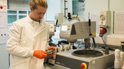
The Thermo Scientific Apreo FEG-SEM offers high-performance imaging and X-ray analysis. The ultimate spatial resolution is approximately 1 nm. Resulting from developments in low-voltage imaging technology, the Apreo can image beam-sensitive materials at accelerating voltages as low as 200 V and a current of 1.6 pA.
This enables high quality imaging of nanomaterials, plastics/polymers and other beam-sensitive materials, such as perovskites. The Apreo chamber has also been designed to allow for large specimens to be examined, useful for industrial component analysis.
The Thermo Scientific ChemiSEM Technology provides a unique live elemental imaging capability, with quantified EDS compositional information being readily and quickly accessed through an easy-to-use interface. A range of external and in-lens detectors can display secondary, backscattered electron and EDS imaging simultaneously, giving excellent resolution across a wide range of accelerating voltages and providing a combination of analyses allowing a rapid assessment of material.
The JEOL JSM-7100F is a highly versatile, easy-to-use analytical field emission gun scanning electron microscope (FEG-SEM). It has a spatial resolution of 1.2 nm at 30 kV. The MSSU microscope is fitted with a ThermoScientific triple analysis system, featuring an UltraDry EDS detector, a MagnaRay parallel beam WDS spectrometer and a Lumis system for electron backscatter diffraction (EBSD).
All three analytical functions are integrated into a single ThermoScientific data system called Pathfinder to allow integration between these three complementary techniques.
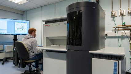
The ThermoScientific Talos 200Fi is capable of both transmission (TEM) and scanning transmission (STEM) analysis. It is equipped with a high brightness FEG source (XFEG) and a high-resolution XTWIN lens, allowing single angstrom imaging resolution.
Images are captured on a direct-electron detector camera (Ceta 16M, with up to 4k x 4k pixels) and smart acquisition routines, such as drift-compensated frame integration.
In STEM mode, a Panther segmented STEM detector allows five simultaneous imaging modes, with complementary morphological and structural information about the sample. Elemental information can be mapped with nearly atomic resolution using a Dual X EDX system, which also designed for efficient collection during tomography.
Thermo Scientific K-Alpha XPS instrument is equipped with a monochromated Al ka X-ray source and variable spot size between 30 and 400 µm. Depth profiling is performed using Thermo's MAGCIS dual-mode monatomic and gas cluster ion source, enabling rapid profiling through inorganic and organic materials.
The 180° double focusing hemispherical analyser with 128-channel detector delivers excellent signal-to-noise spectra, enabling a high throughput of samples whilst also generating high quality chemical state information.
The Advantage software offers state-of-the-art peak fitting of the core level spectra and rapid, accurate qualification of the chemical composition.
The Theta Probe is specifically designed to offer parallel angle resolved XPS (PARXPS) capability enabling the acquisition of non-destructive depth profiles of thin films. This instrument also offers a small spot (15-400 µm) capability for its monochromated Al ka X-ray source and an argon ion gun for depth profiling.
The instrument is also equipped with a preparation chamber which may be used for a range of in-situ (e.g. fracture stage) and other in-vacuo sample preparation procedures.
A ToF-SIMS instrument incorporating a polyatomic Bi ion source offering excellent sensitivity, high spatial and good mass resolution capabilities. Additional Cs and C50 ion sources are installed on this instrument as sputter depth profiling sources although they may also be employed as analysis sources. The instrument offers an ultimate spatial resolution of <100 nm and detection limit of <10 ppm.
Our ToF-SIMS V includes a preparation chamber which may be used for a rnage of in-situ and in-vacuo experiments and sample preparation procedures. In-situ stages for impact and controlled strain rate testing of materials are currently installed on the preparation chamber. The instrument also possesses heating and colling stages in the entry lock and analysis chamber.
Our Bruker Dimension Edge AFM system offers the low drift and low noise capabilities to deliver high quality topographical information in minutes. This instrument includes the PeakForce tapping mode, enabling simple and accurate analysis of delicate samples and various analytical modes, such as conductive AFM imaging and Kelvin Probe measurements.
The ScanAsyst imaging includes integrated visual feedback and pre-configured settings enabling high quality results to be rapidly and simply recorded.
The Bruker DektakXT stylus profilometer is an advanced stylus profilometer that offers a height measurement sensitivity of 4 Å over a distance of up to 160 mm. The integrated software collects accurate step height and quantifies surface roughness, ideal for rapid thin film and sputter crater measurements.
Easy to use top-range digital optical microscope with variable magnification up to 4000x. Can be operated using reflected or transmitted light. Variety of segmented coaxial or ring lamp illumination with 3-axis stage movement to provide larger area high resolution tile scans and/or 3-D information.
Polarising and Differential Image Contrast (DIC) options available. Post processing options for dimensional measurements, contamination/grain size/shape analysis. Surface topology, including waviness and roughness, can be investigated.
The unit has cutting equipment to prepare specimens of various sizes and all material types with high degree of accuracy and minimising any heat affection. We have the ability to mount samples for analysis in epoxy resin, Bakelite thermoset plastic and acrylics.
The samples are then prepared using our modern grinding and polishing kit capable of preparation of metallics, ceramics, polymers, and minerals to a sub-micron finish. The techniques we employ include semi-automatic grinding and polishing on an array of abrasive clothes and discs. We have vibro-polishing which is perfect for improving EBSD pattern quality and more. All performed by highly trained metallographic preparation technical staff. We can also chemically etch for microstructural analysis. All such work is performed by technical staff trained in metallographic preparation.
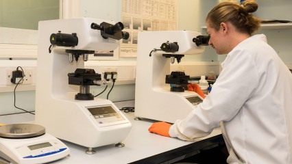
We have a variety of hardness testing apparatus which can support industry clients in a range of applications from failure analysis to quality assurance testing. We have the capability to perform both macro and micro Vicker’s hardness testing, Knoop hardness testing, and Rockwell hardness testing.
Please talk to a member of the team if you want to discuss specific applied loads during testing.

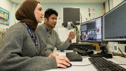
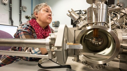
Our Apreo 2 Scanning Electron Microscope being operated by two postgraduate researchers investigating single crystal perovskites.

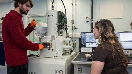
Our JEOL JSM-7100F Scanning Electron Microscope being operated by two postgraduate researchers investigating cast iron microstructure.

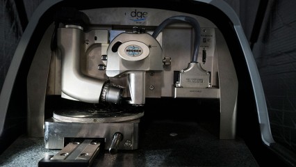
Our Theta Probe X-ray Photoelectron Spectrometer with monochromated aluminium X-ray source.

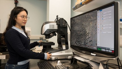
Our Keyence Optical Microscope for rapid imaging of a range of materials. Here a postgraduate researcher is looking at graphite flakes in cast iron.

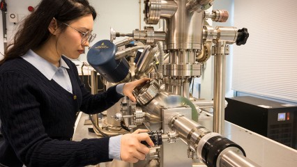
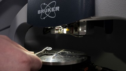
Our ToF-SIMS instrument being operated by a postdoctoral researcher using a bismuth ion source.

Our Quorum sputter coater which we can use to improve an insulators conductivity for electron microscopy observation. Our typical sputter targets are gold, gold/palladium, chromium and silver.
Find an expert
If you would like to use our services then please email our laboratory managers to discuss your problem. Alternatively, join us on LinkedIn, questions and queries are welcome.

Professor Mark Baker
Director of MicroStructural Studies Unit and Surface Analysis Laboratory

Dr Steven Hinder
Surface Analysis Laboratory Manager

Dr Vlad Stolojan
Expert in TEM

James Whiting
MicroStructural Studies Unit Manager