Spin-orbit interaction in InSb nanodevices for quantum technology applications
This project aims to investigate and develop InSb-based devices for quantum technology applications. Direct-write fabrication techniques are being developed for fast prototyping of nanodevices from InSb heterostructures as well as investigation of quantum transport in quantum wells.
Biography
Daisy Shearer is a PhD candidate in experimental condensed matter physics at the University of Surrey’s Advanced Technology Institute, working within the photonics and quantum sciences group. Their PhD research focuses on semiconductor spintronics and electron spin in InSb-based nanodevices for quantum technology applications.
They hold an integrated master’s degree in physics with first-class honours from the University of Surrey (2014-2018) where their master’s research project involved working in R&D at the Centre for Integrated Photonics developing High-Speed Electroabsorption Modulated Lasers (EMLs) for long-haul telecommunications.
They are a passionate science communicator, and educator with a drive to make STEM more accessible and inclusive, particularly for disabled and neurodivergent people.
Spin-polarization of electrons in InSb-based nanostructures (PhD: 2018-present)
My PhD project is on investigating the initialization of electron spin states for spin injection into quantum technologies through the development of novel direct-write fabrication techniques to create versatile InSb-based spin polarizing devices. This involves a combination of researching quantum transport in InSb quantum wells as well as fabrication and testing of various nanodevices made from said quantum wells, such as quantum point contacts and quantum wires. I’m particularly interested in studying the Rashba interaction and the potential for Majorana Zero Modes in InSb heterostructures.
During my master’s degree, I had the opportunity to carry out research for my dissertation— titled ‘Investigating the DC Opto-electrical & Large Signal Characteristics of Electroabsorption Modulated Lasers' — as part of a 9-month internship at the Centre for Integrated Photonics. The company’s research focused on semiconductor-based Photonic Integrated Circuits (PICs) for telecommunications. The project I was assigned to involved the optimization and development of high-speed Electroabsorption Modulated Lasers. These are a type of PIC consisting of a Distributed Feedback Laser followed by an Electroabsorption Modulator. These devices utilise the Quantum-confined Stark effect to modulate laser output and transmit data down optical fibres. My work involved the measurement of both the DC and high-speed characteristics of these devices as well as the modelling and analysis of eye diagrams. I investigated the physical cause of various saturation modes in measured eye diagrams as well as developing a Matlab program to quantify the amount of saturation.
Indicators of esteem
Early Career Physics Communicator Award
Institute of Physics, June 2021
Three Minute Thesis People’s Choice Award
University of Surrey, June 2021
ATI Research Laureate Award
Advanced Technology Institute, University of Surrey, February 2022
Main current research questions:
Can we utilise the spin-orbit interaction in InSb and related III-V semiconductors to create spin-polarized currents?
Can we make a truly 100% spin-polarized current that can be propagated within materials in a useful way?
In what ways can we use spin-polarized currents for quantum metrology and other technology applications?
What is the optimum quantum point contact geometry for spin polarization?
Can direct-write fabrication methods help advance R&D of semiconductor devices?
Are hybrid semiconductor-superconductor devices suitable candidates for next-generation qubits?
Have we actually observed Majorana fermions or do we just think we have?
How can we physically create topological qubits in solid-state materials?
Teaching
Teaching Assistant roles (2018-present) — Faculty of Engineering and Physical Sciences, University of Surrey
FEPS foundation year laboratory demonstrator ‘Engineering and Physical Sciences Laboratory Project’ module (Autumn term 2020, Autumn term 2021)
Physics level 2 laboratory demonstrator for ‘From Atoms to Lasers’ module (Spring term 2019)
Physics level 1 laboratory demonstrator (Autumn term 2018)
Graduate Certificate in teaching and learning (2021-2022) — Surrey Institute of Education, University of Surrey
Pursuing a part-time course on teaching and learning in higher education alongside my PhD, for professional recognition from the Higher Education Academy (HEA)
Education and Public Engagement module design team member (2021-2022) — Faculty of Engineering and Physical Sciences, University of Surrey
Part of the team designing a new FEPS module for undergraduate students across the faculty. Involved with putting together workshop content and facilitator notes for teaching sessions on public engagement as well as helping design assessments
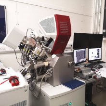
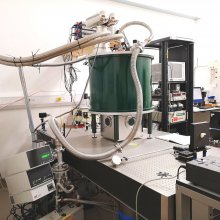
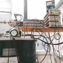
We studied InSb quantum well devices using Landau level tunneling spectroscopy through a three-terminal differential conductance technique. This method is similar to filled state scanning tunneling microscopy but uses a stationary contact instead of a mobile tip to analyze the two-dimensional electron system. Applying magnetic fields up to 15 T, we identified clear peaks in the differential current-voltage profiles, indicative of Landau level formation. By examining deviations from the expected Landau fan diagram, we extract an absolute value for the exchange-induced energy shift. Through an empirical analysis, we derive a formula describing the exchange shift as a function of both magnetic field strength and electron filling. Our findings indicate that the emptying of the í µí¼ = 2 and í µí¼ = 3 Landau levels causes an exchange interaction energy shift in the í µí¼ = 1 level. Unlike prior studies that infer level energies relative to one another and report oscillatory g-factor behavior, our method references the energy of the Landau levels above the filled states of the contact under a bias voltage, revealing that only the ground state Landau level experiences a measurable exchange shift.
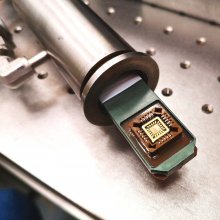
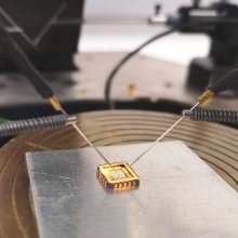
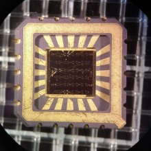
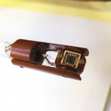
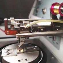
The III-V narrowgap semiconductor InSb has properties such as low effective mass, high mobility, and strong spin-orbit coupling which make it an ideal material for spintronics. Recently there have been numerous device schemes that have been proposed for generating spin polarised currents for spin injection in quantum technologies. At the heart of these schemes is the quantum point contact (QPC) which requires nanoscale lithography and gated structures. Here we present a complete fabrication toolkit that employs focused ion beam (FIB) lithography as a flexible direct-write technique for rapid prototyping of QPCs. Two approaches for fabricating QPCs have been explored. The first method involves defining QPCs using direct etch writing of InSb quantum wells. A FIB assisted XeF2 chemistry has been used to form side gates with air gaps. The second technique uses FIB assisted deposition to form a siloxane gate dielectric, as well as direct-write of metalization using platinum to form split top gates. Compatibility of InSb with these processes has been confirmed by post-fabrication measurements of the electronic properties using Shubnikov de Haas and quantum Hall. The versatility of this direct-write technique makes it ideal as a rapid device prototyping tool.
InSb is a III-V narrow-gap semiconductor with properties such as low effective mass, high mobility, and strong spin-orbit coupling making it an ideal material for applications such as spintronics mid-infrared photonics, and nanoelectronics. InSb quantum wells can be made by growing an InSb/InAlSb structure on a Ga substrate using molecular beam epitaxy. However, it is notoriously difficult to fabricate nanodevices from InSb/InAlSb quantum wells due to factors such as its low thermal budget and the production of non-volatile by-products in conventional etching processes, leading to unwanted deposition of material onto the material surface. Current wet and dry etching techniques take a long time and require expensive lithography masks to make new devices, slowing the development of optimised nanodevices.We investigate focused ion beam (FIB) lithography as a "rapid prototyping" fabrication technique to create semiconductor nanodevices from InSb quantum wells. FIB methods have the advantage of being relatively quick and "maskless", making them ideal for use in the research environment as new iterations of device design can be made quickly and different etching chemistries and electrical properties can be tested in-situ. A variety of Xe plasma FIB parameters were tested to optimise the feature resolution and etching quality of milled trenches at low temperatures. The XeF2 gas-assisted etching process was also studied as an alternative to the Cl2 chemistry that is typically employed for dry etching of InSb. Cross-sections and profiles of the trenches indicate that the XeF2 etch yields superior trench smoothness and mills material from the surface at a much higher rate. This method was also less prone to deposition of unwanted material onto the surface of the sample. This high-resolution fabrication method can be used for the rapid development and optimisation of individual nanoscale devices before mass production.