Dr Radu Sporea is Associate Professor of Power Electronics and Semiconductor Devices at the Advanced Technology Institute (ATI) and a Sustainability Fellow within the University's Institute for Sustainability. Radu recently completed his EPSRC Early Career Fellowship (EP/V002759/1) concerned with developing new energy-efficient electronic devices for future display, edge signal processing, and bio-inspired computation. Prior to this appointment he was Royal Academy of Engineering Academic Research Fellow (2011-2016), EPSRC PhD+ Fellow (2010-2011) and PhD researcher (2006 - 2010) in the same centre. Prior to his time at Surrey, Radu has studied computer systems engineering at “Politehnica” University, Bucharest, Romania, and has worked as a Design Engineer for Catalyst Semiconductor Romania, now part of ON Semiconductor, on ultra-low-power CMOS analog circuits.
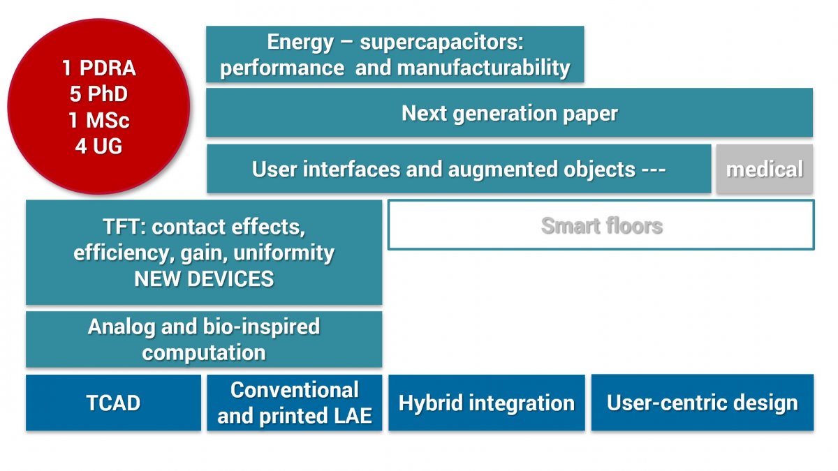
Current research in Radu’s team focuses on three main topics:
Advanced large-area semiconductor device design, including transistors with increased tolerance to fabrication variability, improved energy efficiency and high gain. Analog, bio-inspired and neuromorphic computation are intrinsic features of the hardware building blocks being developed.
Large area sensors and sensor arrays for smart environments, wearables and autonomous sensing, focusing on multi-modal low-cost integration in commercial manufacturing platforms and mass-market products.
Manufacturability and security of hardware systems, including advanced simulation and material-device-circuit interaction.
Radu enjoys travel photography and public engagement in science.
Public engagement in science
Occasionally, Radu will write, present and produce short Science films on YouTube.
His electronic engineering podcast has been featured on Pod Academy. In 2014, Radu was the Academic Minute's resident technology expert.
Radu was a participant in the 2012 edition of Famelab. He has performed on and presented at Pint of Science, Café Scientifique, Science Showoff, Bright Club and Pecha Kucha Guildford. He appeared on BBC4's "Some Boffins with Jokes". He occasionally performs improvised science comedy with Mark Richardson as "Just Enough Doctorate to Perform" at events such as Pint of Science Guildford.
Areas of specialism
Electronic devices and circuits; Flexible and printed electronics; Manufacturability and reliability of electronics; Modelling and simulation; Unconventional electronics; Neuromorphic and bio-inspired computation
University roles and responsibilities
Leading the Flexible Electronics pillar of ATI research
Research covers aspects of electronic devices from functional nanomaterials and active devices, to simulation and modelling circuits, and large-area systems.
The core activity is represented by power-efficient, cost-effective large-area electronics in organic and inorganic semiconductor technologies. Most of the work is based on the concept of source-gated transistor(SGT), a device invented at Surrey by Prof Shannon and collaborators. Previous results in polysilicon and amorphous silicon devices highlight the performance benefits of SGTs: higher amplification and lower energy requirements in certain circuit configurations.
Now, using solution-processed semiconductor technologies we aim to create large-area flexible and possibly transparent electronic circuits which are very resilient to process variations and can be made without the complex tools required by conventional material deposition and photolithography processes.
The multimodal transistor, invented together with Dr Eva Bestelink, is the evolution of the original SGT concept, with superior functional, energy, and reliability features for next-generation display, edge processing, and bio-inspired computing applications.
The device/circuit fabrication activity is complemented by computer simulation and modelling of device physics and circuit design using the SILVACO suite (Atlas, Athena, MixedMode) for analoguwe and mixed signal applications.
Academic collaborations (restricted for confidentiality)
General topics for future UG, Msc and PhD projects
Paper-based electronics and unconventional user interfaces
Analog computation, near-zero-power electronics, hardware learning and AI
Organic and inorganic advanced devices and circuits for sensors and IoT
Simulation and modelling of electronic devices and circuits
Reliability and manufacturability of electronic devices and circuits
Joining the team
I am looking for dedicated and ambitious individuals to join my team. Please email to discuss. Attach a CV, specify your interest and availability to join. Highlight achievements that you are particularly proud of, and write a short paragraph on your ideal research project at Surrey.
Radu was University of Surrey's 2017 Early Career Teacher of the Year. In 2018, he was presented the Department of Electrical and Electronic Engineering Tony Jeans Inspirational Teaching Award.
Undergraduate admissions
Admissions matters are now handled by Dr Lucia Florescu, admissions tutor, and by Dr Kai Yang and Prof. David Carey.
Ad-hoc tutorials
Please email to arrange a convenient time to meet. Briefly outline the topics for discussion.
Teaching modules
Energy generation and conversion is a topic of great interest, considering the rise of electrical vehicles, sustainable energy sources, and data centre power requirement. The module I currently teach deals with the basics of energy conversion together with signal amplification, serving as a basis for in-depth studies for those who wish to pursue a career in this dynamic field.
Final year research projects and MSc projects in low-power and sustainable electronics, device and circuit simulation, bio-inspired and neuromorphic computing, electronics manufacturability, and user interfaces.
This study aims to contribute to the burgeoning field of brain‐inspired computing by expanding it beyond conventional fabrication methods. Herein, the obstacles toward the effective inkjet printing process are encountered and the electrical characteristics are explored, providing new insights into the reliability aspects of fully printed Ag/a‐TiO2/Ag electronic synapses. The versatility of the approach is further enhanced by the highly stable in‐house‐developed a‐TiO2 ink, exhibiting optimal shelf life of five months and repeatable jetting, producing layers with nanoscale thickness resolution. Most importantly, device electrical characterization reveals synaptic dynamics, leading to activity‐dependent conductance state retention and adaptation characteristics, implying inherent learning capabilities. The synaptic dynamics are attained by solely adjusting the duty cycle of the applied pulsed voltage trigger, while keeping amplitude and polarity fixed, a method readily compatible with realistic applications. Furthermore, I–V analysis demonstrates a dynamic range dependence on a‐TiO2 layer thickness and conduction mechanism that is akin to the conventionally developed electronic TiO2 synapses. The developed devices provide a time‐ and cost‐effective ecologically benign alternative toward biomimetic signal processing for future flexible neural networks.
This work demonstrates the benefits of low, but dominant, contact barriers in organic thin-film transistors (OTFTs) for threshold stability. Multimodal transistor measurements (≤ -8 V) confirm contact-controlled operation even when single-gate OTFTs produce apparent Ohmic behavior (dVSAT / dVGS ≈ 0.85). Simulations demonstrate that the contact-controlled nature of the device (contact energy barrier ΦB = 0.4 eV for hole mobility 2.7 cm2V-1s-1) promotes drain current stability with respect to interface charge-induced threshold variations, a finding with direct implications on emerging OTFT applications, e.g. displays, where simplified pixel design may lead to competitive new implementations. The stability and saturation properties also make such devices attractive to life sciences and distributed sensors applications.
The Arthritis patients and aging population has challenged society to develop safer, independent living environments. Falls, associated injuries, and delays in fall treatment are major causes of morbidity and death in older adults. Therefore, fall detection systems are fundamental to reducing fall risks and building safer environments. Designing fall detection systems is an emerging field of research. The development of the system relies on a sensing mechanism, processing unit, and communication to alert the emergency facilities. Each module is crucial in providing a cost-effective, accurate, reliable, and robust solution. Technological advancements in fall detection systems, particularly wearable and non-wearable devices, offer promising solutions. Wearable systems are prevalent due to their cost-effectiveness and ease of installation, but they canbe unreliable if not worn consistently. Non-wearable systems, including smart flooring, provide continuous monitoring but are expensive and complex to maintain. This article reviews the development and deployment of fall detection technologies, examining their practical limitations and emphasizing floor-based detection systems as a viable solution for fostering independent living among older adults.
David M. Frohlich, Haiyue Yuan, Emily Corrigan-Kavanagh, Elisa Mameli, Caroline Scarles, Radu Sporea, George Revill, Alan W. Brown, Miroslaw Bober (2024)A Market-Ready Ecosystem for Publishing and Reading Augmented Books, In: J Wei, G Margetis (eds.), HUMAN-CENTERED DESIGN, OPERATION AND EVALUATION OF MOBILE COMMUNICATIONS, PT II, MOBILE 202414738pp. 58-75 Springer Nature
Many studies show the possibilities and benefits of combining physical and digital information through augmented paper. Furthermore, the rise of Augmented Reality hardware and software for annotating the physical world with information is becoming more commonplace as a new computing paradigm. But so far, this has not been commercially applied to paper in a way that publishers can control. In fact, there is currently no standard way for book publishers to augment their printed products with digital media, short of using QR codes or creating custom AR apps. In this paper we outline a new publishing ecosystem for the creation and consumption of augmented books, and report the lab and field evaluation of a first commercial travel guide to use this. This is based simply on the use of the standard EPUB3 format for interactive e-books that forms the basis of a new 'a-book' file format and app.
Contact resistance is traditionally regarded as an obstacle to be eliminated in transistors, limiting the charge injection across a wide range of semiconductors. Here we show that controlled variations in contact resistance, induced by asymmetric electrode geometry, can be exploited as a design parameter rather than treated as a drawback. Using ZnON/DNTT heterojunction antiambipolar transistors (AATs), we show that electrode placement defines distinct current pathways and enables multiple Gaussian-like transfer curves within a single device platform. Combining four electrode layouts with dual operating modes yields eight distinct Gaussian-like transfer profiles. This expanded functionality demonstrates that contact engineering enables tunable analog responses directly relevant to neuromorphic computing. The ability to adjust Gaussian amplitude, position, and width provides hardware-efficient implementations of activation functions, continuous weight representations, and probabilistic processing. Based on the obtained Gaussian responses, reinforcement learning tasks such as Duffing oscillator prediction and power consumption forecasting are performed, illustrating the applicability of AATs to nonlinear dynamic systems.
A neuromorphic optical synapse transistor based on a spectrally tuned floating-gate synapse (STFGS), designed to achieve optoelectronic synaptic behavior, is presented. The device incorporates a heterojunction structure composed of a dinaphtho[2,3-b:2',3'-f]selenopheno[3,2-b]selenophene (DNSS) upper channel and an E)-2-(2-((6-(di-p-tolylamino)-4,4-dimethyl-4H-indeno[1,2-b]thiophen-2-yl)methylene)-3-oxo-2,3-dihydro-1H-inden-1-ylidene)malononitrile (Dta-Inth-IC) floating-gate layer. A parylene dielectric layer strategically positioned between the DNSS and Dta-Inth-IC layers functions as a barrier, enabling selective charge storage within the floating-gate architecture. Synaptic plasticity is analyzed by varying stimulation conditions, such as the on-time, off-time, and pulse number of optical pulses. Long-term potentiation (LTP) is observed with efficient charge trapping in the floating-gate under 660 nm light stimulation. Energy band alignment analysis confirms charge accumulation in Dta-Inth-IC under 660 nm light, while 455 nm light stimulation induced rapid recombination in DNSS. The applicability of artificial neural networks (ANN) based on the potentiation curves obtained from STFGS is evaluated. For this purpose, a convolutional neural network (CNN)-based ANN is designed and performs classification tasks using the Fashion Modified National Institute of Standards and Technology (Fashion MNIST) dataset. Through repeated training, a maximum recognition rate of 91.37% for 660 nm light stimulation is achieved, demonstrating that the STFGS successfully mimics synaptic behavior.
A source-gated transistor (SGT) is a type of thin film transistor (TFT) with unique behaviors. Functionally, the SGT is designed to decrease the saturation voltage at a lower and often more stable saturation current in comparison to a standard TFT, which makes it preferable in some circuit applications. This is achieved by introducing additional effects especially around the source region which differentiate the SGT enough that it cannot be described by a standard TFT compact model. The work presented aims to create the first empirical SGT compact model which may be implemented in DC circuits. This compact model has been developed using the data obtained from an SGT TCAD model.
We investigate a mechanism for greatly improving switching speed in contact-controlled thin-film transistors (TFTs), which have persistently performed much slower than Ohmic contact variants. Separating the mechanisms for charge injection and conduction can result in transient settling times two orders of magnitude lower than existing contact-controlled devices (e.g. source-gated transistor) and even lower than in Ohmic contact TFTs for a given drain current. High speed operation is not necessarily only promoted by the well-studied reduction in contact resistance, but rather by a presence of a pre-charged accumulation layer in the source region. These findings greatly expand the applicability of contact-controlled transistors.
— We present the first physical compact model for an amorphous Silicon source-gated transistor with variable Schottky barrier height. A previously published empirical compact model and TCAD model of a source-gated transistor are used to identify dominant effects present. The compact model is then validated on real device measurements. The compact model aims to operate under common conditions and typically desirable regimes of operation for a source gated transistor, such as the flat saturation regime occurring at a particularly low saturation voltage. The dominant injection mechanisms occur through thermionic and thermionic-filed emission, which are the contact effects present in a source-gated transistor. Thermionic emission tends to be dominant under most common conditions. The model is suitably accurate to be used as a representation of a source-gated transistor in a SPICE simulation. This can be seen as a first step toward analog circuit design with source-gated transistors as compact models enable circuit designers to utilize new and unique devices.
Contact-controlled transistors are rapidly gaining popularity. However, simply using a rectifying source contact often leads to unsatisfactory operation, merely as a thin-film transistor with low drain current and reduced effective mobility. This may cause otherwise promising experiments to be abandoned. Here, data from literature is analyzed in conjunction with devices that have been recently fabricated in polysilicon, organic and oxide semiconductors, highlighting the main factor in achieving good saturation, namely keeping saturation coefficient gamma well below 0.3. Secondary causes of suboptimal electrical characteristics are also discussed. Correct design of these alternative device structures will expedite their adoption for high gain, low-frequency applications in emerging sensor circuits.
As oxide semiconductors increase in popularity with emerging flexible electronics, advances in material performance may lead to parasitic and nonideal effects becoming more prominent. Specifically, in source-gated transistors (SGTs), and other contact-controlled devices, the influence of the lateral drain field produced by drain bias leads to an overwhelming increase in charge density at the source edge and obliterates their signature flat saturation at low drain voltages. Here, we present high current density amorphous InGaZnO (a-IGZO) SGTs in a bottom contact architecture using Pt source and drain electrodes. The devices were fabricated by ensuring an oxygen-rich atmosphere to prevent the formation of oxygen vacancies at the Pt/a-IGZO interface. Incorporating a field relief structure within the source contact improves drain current saturation, toward behavior predicted by the saturation coefficient. In the device architecture considered, the screening was less effective for a field plate insulator thickness under 30 nm, possibly due to increased tunneling. Field plate incorporation is one of the strategies that ensures flat saturation and the suitability of contact-controlled transistors for a multitude of current driving and amplification applications.
Artificial neural networks (ANNs) providing sophisticated, power-efficient classification are finding their way into thin-film electronics. Thin-film technologies require robust, layout-efficient devices with facile manufacturability. Here, we show how the multimodal transistor's (MMT's) transfer characteristic, with linear dependence in saturation, replicates the rectified linear unit (ReLU) activation function of convolutional ANNs (CNNs). Using MATLAB, we evaluate CNN performance using systematically distorted ReLU functions, then substitute measured and simulated MMT transfer characteristics as proxies for ReLU. High classification accuracy is maintained, despite large variations in geometrical and electrical parameters, as CNNs use the same activation functions for training and classification.
The development and optimization of flexible electronics has allowed technology to be better integrated in applications and environments where the physically rigid nature of electronics is previously a limiting factor. Printing techniques contribute to lowering the fabrication costs and making manufacturing-on-demand viable. The use of flexible electronics in the user interface domain has been previously explored with solution-processed optical photodetectors created and the feasibility of using flexible sensors demonstrated in augmented paper applications. In this work, low-cost photodetectors are developed using scalable printing techniques, their electrical performance is analyzed, and their stability over time is studied both in air and in vacuum, the structure is optimized through a combinatorial optimization experiment, and a scalable integration method is demonstrated for creating larger, addressable arrays of detectors. This is a demonstration of how printing methods allow for easy, cost-effective, and low-energy manufacturing of uniform and stable photosensors.
Eva Bestelink, Giulio Galderisi, Patryk Golec, Yi Han, Benjamin Iniguez, Alexander Kloes, Joachim Knoch, Hiroyuki Matsui, Thomas Mikolajick, Kham M. Niang, Benjamin Richstein, Mike Schwarz, Masiar Sistani, Radu A. Sporea, Jens Trommer, Walter M. Weber, Qing-Tai Zhao, Laurie E. Calvet (2024)Roadmap for Schottky barrier transistors, In: Nano futures8(4)042001 IOP Publishing Ltd
In this roadmap we consider the status and challenges of technologies that use the properties of a rectifying metal-semiconductor interface, known as a Schottky barrier (SB), as an asset for device functionality. We discuss source gated transistors, which allow for excellent electronic characteristics for low power, low frequency environmentally friendly circuits. We also consider reconfigurable field effect transistors. In such devices, two or more independent gate electrodes can be used to program different functionalities at the device level, enabling ultra-secure embedded devices. Both types of transistors can be used for neuromorphic systems, notably by combining them with ferroelectric SB transistors which enable a large number of analog states. At cryogenic temperatures SB transistors can advantageously serve for the control electronics in quantum computing devices. If the source/drain of the metallic contact becomes superconducting, Josephson junctions with a tunable phase can be realized for scalable quantum computing applications. Developing applications using SB devices requires physics-based and compact models that can be used for circuit simulations, which are also discussed. The roadmap reveals that the main challenges for these technologies are improving processing, access to industrial technologies and modeling tools for circuit simulations.
Emerging micro light-emitting diode (microLED) displays promise high brightness, improved lifetime, and high pixel density. However, to achieve the desired color accuracy, microLEDs require constant current driving, which can result in wavelength shift at higher pixel brightness. This presents a challenge for pixel circuit design. The driving scheme must vary the emission duration (i.e., pulse width modulation, PWM) to prevent wavelength shift, and it must also include an element of current magnitude control (pulse amplitude modulation, PAM) for fine tuning. This results in complex signaling, large footprint, and multiple sources of variability arising from the numerous transistors, which together diminish the implementation's efficacy. Here, we present a 6T1M2C pixel circuit, which takes advantage of the properties of the multimodal thin-film transistor (MMT) to achieve PWM and PAM simultaneously, rather than in a hybrid configuration, while also performing threshold compensation. The MMT is the first transistor that allows for separation of injection (current magnitude) from channel conduction state (timing), allowing a higher degree of freedom for designing pixel circuits with lower complexity. This proof-of-concept TCAD implementation demonstrates the benefits of MMT-based simultaneous PWM and PAM circuits, with compact device footprint, reduced circuit complexity, and power-efficient features.
This study aims to increase the output current of the a-IGZO source-gated transistor (SGT) through TCAD
simulation and experiment. As SGT proves to be useful in various low-power applications and wearable
devices, the low output current characteristics limit the adaptability of this structure. It is estimated that
a higher level output current is achievable by optimizing this architecture while retaining fast saturation
characteristics. The SGT structure simulations have been performed with adjusted density- of-states (DoS)
parameters from experiments; this made TCAD simulation more realistic and can be used to predict the
results of fabricated SGTs. The results from this study show that longer source-channel overlap and thinner
channel is preferable; the SGT with longer source-channel overlap will result in the Mode II injection
dominating over the Mode I injection. The Mode I injection occurs at the edge of source contact near the
channel region, while the Mode II injection occurs at the bulk of the source at the farthest region from the
channel. The result from experiment shows that the fabricated SGT exhibits Mode II injection
characteristics-that is the current will increase linearly with increasing gate voltage. From this study. it
could be concluded that the source-channel overlap of 210 µm with a channel thickness of 20 nm and
channel length of 5 µm is the optimized structure that could provide high output current with little
temperature dependence. Further improvement of the output current could be achieved by utilizing lower
work function source metal.
Printed amplifiers are promising components for flexible and wearable devices. The circuits need to have small footprint, high amplification, and low power consumption, which is not simultaneously possible with conventional thin-film transistors because multiple stages are required and introduce sources of variability, failure, or wasted area. Source-gated transistors (SGTs) can in principle have extremely high intrinsic gain but this is not always the case because of lateral field control problems. A good solution is the use of field plate structures, which are straightforward to implement with top contacts but not so with bottom contacts. Here, a printed implementation of organic SGT with a field plate is presented, which can achieve a record high intrinsic gain of 920 V/V. The single-stage common-source amplifier with two organic SGTs also exhibits a high gain of 700 V/V. Simulations confirm the effectiveness of the printed field plate, making it a promising approach for future flexible and wearable electronics.
Even though a plethora of printing technologies are currently available and their potential for the fabrication of low-cost and flexible sensors has been widely investigated, systematically based, and statistically sustained comparative studies are missing in the literature. In this work, we compare screen, inkjet, and dispense printing for the fabrication of carbon nanotube (CNT)-based ammonia (NH3) chemiresistive flexible gas sensors for the first time. Moreover, we report the first CNT-based gas sensor fabricated via Voltera printer. The devices were made of a thin layer of spray-coated CNTs and printed silver-based interdigitated electrodes. To draw a thoughtful comparison the same sensor layout, materials, and fabrication flow were used. The device morphological features were acquired through microscopic, atomic force microscope, and 3D images; additionally, the response to NH3 as well as the printing process characteristics for each technique was analyzed. From 300 & mu;m nominal spacing between lines, we obtained a decrease of 25%, 13%, and 5% on the printed spacings with dispense, screen, and inkjet printing, respectively. At 100 ppm of NH3, a maximum response of 33%, 31%, and 27% with the dispense-, inkjet-, and screen-printed sensors were found, respectively. Statistical differences were observed between the mean values on the NH3 response of dispense- compared to the inkjet- and screen-printed sensors, which in effect showed the highest response in the Tukey test. This demonstrated that the fabrication technique employed can induce a different response mainly driven by the printed outcomes. Following a holistic approach that includes the sensor response, the application, the market perspective, and the process versatility, we suggest screen printing as the most suitable method for CNT-based NH3 gas sensor fabrication.
Thin-film transistors with a split gate structure have been continuously studied for integration into future electronic devices. By introduction of a gate gap, a thin-film transistor can perform various logic circuit operations within the single channel region. However, the impact of the gate gap on the electrical characteristics of split gate thin-film transistors has not been well investigated. In this study, we fabricated and characterized split gate thin-film transistors to realize logic OR and AND operations and conducted technology-aided computer design simulations with Silvaco Atlas simulations for logic AND implementation. Using technology computer-aided design simulations, we systematically analyzed the impact of the gate gap on the overall device characteristics as well as electric fields, energy bands, and carrier concentrations with cutlines in the channel region. Furthermore, we implemented the split gate transistor on a flexible paper substrate, demonstrating its possibility through up to 1000 bending cycle tests and indicating its potential for integration into more advanced electronic devices.
We propose a 5-transistor, 2-capacitor (5T2C) AMOLED pixel circuit using a multimodal transistor (MMT) as driver, which may be more appropriately referred to as 4T1M2C to reflect the inclusion of a device which is distinctly different from conventional Ohmic-contact thin-film transistors (TFTs). The MMT is a type of contact-controlled transistor, here implemented with a Schottky source. Its gating mechanisms separate ‘analog' charge injection, controlled by the source contact, from ‘digital' channel conductance switching. The mixed-signal operation of the MMT allows it to perform the function of multiple conventional transistors in a power- and area-efficient manner, enabling pixel circuit design to achieve superior image uniformity and energy efficiency, due to the combination of threshold compensation scheme and inherent saturation properties of the MMT drive transistor.
Low-temperature microcrystalline silicon ( μ -Si) has been realized in a Corial inductively coupled plasma chemical vapor deposition (ICP-CVD) system. Both doped and undoped μ -Si layers have been investigated in terms of resistivity and crystalline fraction. Following a μ -Si recipe using H 2 /Ar/SiH 4 mixture developed for plasma-enhanced chemical vapor deposition (PECVD), a technological transfer has been carried out in ICP-CVD. Some key parameters have been defined and a domain of use determined for N-type, P-type, and intrinsic layers. In the same reactor, nitride layers have also been deposited to perform gate insulator for thin-film transistors (TFTs). Finally, TFTs were fully realized by ICP-CVD and also electrically characterized, highlighting the interest of ICP-CVD for thin-film electronics. This demonstrates the great versatility of ICP-CVD technology applied to low-temperature electronic processes.
With growing interest in organic phototransistors, as not only sensors but also neuromorphic computing elements, the vast majority of research investigates structures comprising Ohmic source/drain contacts. Here, it is shown how source-gated transistors (SGTs), in which a source contact barrier dominates electrical characteristics, can be implemented as phototransistors. Organic photo-SGTs (OPSGTs) based on vacuum-processed small-molecule dinaphtho[2,3-b:2′,3′-f]thieno[3,2-]thiophene (DNTT) demonstrate low saturation voltage, exceptional tolerance to channel length variation, and photo-to-dark current ratio (PDCR) peaks over 106 for 819 µW broad spectrum incident light power. At zero gate-source voltage, the PDCR reaches 104, showing promise for simple sensor circuit implementation in medical and wellbeing applications.
We report the first implementation of a complementary circuit using thin-film source-gated transistors (SGTs). The n-channel and p-channel SGTs were fabricated using the inorganic and organic semiconductors amorphous InGaZnO (IGZO) and dinaphtho[2,3-b:2 & PRIME;,3 & PRIME;-f]thieno[3,2-b]thiophene (DNTT), respectively. The SGTs exhibit flat output characteristics and early saturation (dV(DSAT)/dV(GS) = 0.2 and 0.3, respectively), even in the absence of lateral field-relief structures, thanks to the rectifying source contacts realized with Pt and Ni, respectively. Hence, the complementary inverter shows excellent small-signal gain of 368 V V-1 and noise margin exceeding 94% of the theoretical maximum. We show that the trip point of such inverters can be tuned optically, with interesting applications in compact detectors and sensors. Numerical simulation, using Silvaco ATLAS, reveals that optimized and monolithically-integrated SGT-based complementary inverters may reach a small-signal gain over 9000 V V-1, making them highly suited to low and moderate speed digital thin-film applications. This proof-of-concept demonstration provides encouraging results for further integration and circuit level optimizations.
Organic Source‐Gated Phototransistors with > 104 Photo‐To‐Dark Current Ratio
Contact‐controlled transistors versatile thin‐film devices have promising potential in emerging sensors and user interfaces. The most mature of these, source‐gated transistors (SGTs), have excellent signal gain and uniformity characteristics. In article 2301931, Hagen Klauk, Radu A. Sporea, and co‐workers demonstrate organic SGTs fabricated using organic semiconductor DNTT, with superior geometrical and temporal stability. These structures show high sensitivity to blue light in a simple‐to‐implement, robust architecture, and the functionality can be generalised to numerous topical areas, including low‐cost light sensors for wellbeing, health, and environmental applications.
A multiple-gate transistor comprises a source, a drain spaced apart from the source, a semiconductor region disposed between the source and drain, and an insulating region disposed over the semiconductor region. A current control gate controls a magnitude of current flowing between the source and drain through the semiconductor region in dependence on a first electric field applied to the current control gate, and is separated from the source by the semiconductor region and the insulating region. A switching gate permits current to flow between the source and drain through the semiconductor region in dependence on a second electric field applied to the switching gate. The transistor's conduction state can be controlled by varying the second electric field applied to the switching gate, whilst varying the first electric field that is applied to the current control gate can set the magnitude of the current through the multiple-gate transistor.
We report the first In-Ga-Zn-O source-gated transistors on a flexible polyimide film. Our findings show that using Au contacts and the incorporation of an ultrathin SiO 2 tunnel layer facilitate contact-controlled operation, distinct from conventional thin-film transistors with Ti contacts. This was confirmed by early saturation in the output characteristics and the very low saturation voltage change over a gate voltage change of < 0.1 V/V which agrees well with the theoretical saturation coefficient of ≈ 0.1.
In today's digital world, paper's reason of being is challenged. Yet, studies suggest that books and paper-based objects have advantages ranging from the tactile sensation to information retention and indexing. We have developed a hybrid electronic device, the "a-book," that offers access to up-to-date and pertinent multimedia content as part of the ordinary interaction with a typical hardcover book. The device maintains the look and feel of a conventional book and is connected to the web through an adjunct smart device. Here, we provide a technical project summary of the electronic system for book augmentation. We outline the system's functionality and discuss its manufacturability, prospects, and limitations in the context of current and emerging flexible electronics technologies.
Recently, hybrid organic-inorganic perovskites have emerged as promising photo-sensing materials for next-generation solution-processed phototransistors, achieving high responsivity, detectivity, and fast response. Here, a phototransistor that can detect visible light using a low-cost, solution processed methylammonium lead iodide/zinc oxide (CH3NH3PbI3/ZnO) heterostructure is reported. While typical ZnO thin-film transistors (TFTs) do not show any photocurrent under visible light illumination, CH3NH3PbI3 (MAPbI(3)) coated ZnO TFTs exhibit substantial photocurrent. Additionally, the optical, morphological, and structural characteristics of the light-absorbing layers are further controlled by altering the precursor ratio of methylammonium iodide and lead (II) iodide (MAI:PbI2), which in turn affects the photosensitivity. Stoichiometric composition (MAI:PbI2 = 1:1) of MAPbI(3) demonstrates optimal characteristics with a responsivity of 234 A/W and a high detectivity of 3.74 x 10(13) Jones under white light illumination. The high photo-responsivity and detectivity result from the combination of the suitable optoelectronic properties of the stoichiometric MAPbI(3) film and its smooth interface with the ZnO channel.
A Corial Inductively Coupled Plasma Chemical Vapor Deposition (ICP‐CVD) system has been investigated to produce un‐doped and doped μ‐Si layers, as well as insulators, leading to a general capability of performing N and P type TFTs. This enables to develop rapid prototyping of TFTs. Resistivity of layers and TFT issues from ICP‐CVD have been electrically characterized.
A new device, the Multimodal Transistor (MMT), separates charge injection from conduction. With design optimization, it can achieve a constant transconductance with independent on/off switching of output current. This functionality has ample applications in energy efficient analog computation and hardware learning.
Self-aligned Schottky-source source-gated transistors (SGTs) have been made in polysilicon. The structures enable a direct comparison to be made between a SGT and a standard thin-film field-effect transistor (FET) on the same device. SGTs having excellent characteristics have been fabricated, with intrinsic gains approaching 10,000. The effects of bulk doping in the polysilicon and of the source barrier modification implant are considered in the context of the electrical output characteristics. It is shown that the choice of source length is a tradeoff between device speed and current uniformity.
The characteristics of laser diodes (wavelength of the emitted radiation, output optical power, embedded photodiode photocurrent, threshold current, serial resistance, external quantum efficiency) are strongly influenced by their driving circumstances (forward current, case temperature). In order to handle such a complex investigation in an efficient and objective manner, the operation of several instruments (a laser diode driver, a temperature controller, a wavelength meter, a power meter, and a laser beam analyzer) is synchronously controlled by a PC, through serial and GPIB communication. For each equipment, instruments drivers were designed using the industry standards graphical programming environment - Lab VIEW from National Instruments. All the developed virtual instruments operate under the supervision of a managing virtual instrument, which sets the driving parameters for each unit under test. The manager virtual instrument scans as appropriate the driving current and case temperature values for the selected laser diode. The software enables data saving in Excel compatible files. In this way, sets of curves can be produced according to the testing cycle needs.
Georgios Bairaktaris, Brice Le Borgne, Sirpa Nordman, Samuli Yrjänä, Vikram Turkani, Rudresh Gosh, Vahid Akhavan, Peter Bagge, Timo Turpela, David M Frohlich, Radu A Sporea (2020)78‐2: Using Physical Books as Interfaces to Digital Displays, In: SID International Symposium Digest of technical papers51(1)pp. 1159-1162
A new form of interaction with digital displays is described, using the pages and binding of a physical book as the interface. This leads to a form of augmented book, or a‐book, which can seamlessly trigger multimedia content on a nearby device using embedded light, pressure or touch sensors.
The successful commercialization of organic field-effect transistors (OFETs) for advanced integrated organic electronics requires reducing device sizes, which inevitably clashes with the constraints imposed by the contact effects. Herein, it is demonstrated that the contact resistance in OFETs based on monolayer organic semiconductors is extremely low, especially at mild biasing conditions. The contributions of the access resistance and the metal-organic interface resistance are successfully disentangled for the first time. It is shown that, contrary to the conventional view, the contact resistance of monolayer OFETs in the saturation regime exhibits a very weak dependence on the source electrode length. In the monolayer OFETs based on 2,9-didecyldinaphtho[2,3-6:2',3'-f]thieno[3,2-b] thiophene (C-10-DNTT), a gate-voltage-independent access resistivity (2.2 10(-2) Omega cm(2)) at V-DS = - 1 mV is obtained, while the interfacial metalorganic Schottky contact resistance is found to be negligible. The depletion of a diode associated with the metal-organic interface expands with increasing V-DS and eventually bottlenecks the device performance. Finally, how to overcome such a carrier depletion contact resistance bottleneck and achieve OFETs with outstanding performance are shown. These findings pave the way toward sophisticated organic electronic applications based on the use of monolayer OFETs.
This paper describes some of the performance characteristics of self-aligned polysilicon Schottky Source- Gated Transistors (SGTs) made on glass by laser annealing of amorphous silicon. The threshold and Schottky barrier height are tuned by varying the dose of dopants in the bulk and under the source respectively. These devices are well suited for analog applications owing to their low saturation voltage, low drain field dependence of the current and intrinsic gain which is in excess of 1000 for well designed structures. Double drain operation leads to fT ≈100MHz for non-optimized devices. Index Terms— Source-Gated Transistor, polysilicon, analog
Multimodal transistors (MMTs) build on previous understanding of contact‐controlled transistors. Additionally, they allow precise control of the charge injected, distinct from controlling the state of conduction of the semiconductor channel. This approach leads to interesting functionality, of benefit to displays and other large area electronic circuits. Here, we summarize the construction and functionality of the MMT and outline potential applications.
New materials and optimized fabrication techniques have led to steady evolution in large area electronics, yet significant advances come only with new approaches to fundamental device design. The multimodal thin‐film transistor introduced here offers broad functionality resulting from separate control of charge injection and transport, essentially using distinct regions of the active material layer for two complementary device functions, and is material agnostic. The initial implementation uses mature processes to focus on the device's fundamental benefits. A tenfold increase in switching speed, linear input–output dependence, and tolerance to process variations enable low‐distortion amplifiers and signal converters with reduced complexity. Floating gate designs eliminate deleterious drain voltage coupling for superior analog memory or computing. This versatile device introduces major new opportunities for thin‐film technologies, including compact circuits for integrated processing at the edge and energy‐efficient analog computation.
With the ever-increasing demands for integration of advanced electronic functions into large-area electronics, down-scaling of thin-film transistors (TFTs) becomes very necessary. The key device operational issues associated with TFT scaling, including short-channel effects (SCEs) and self-heating, are considered in this paper. Device structure engineering approaches are introduced to suppress the SCEs for designing short-channel TFTs with excellent digital and analog performance. And electro-thermal simulation results show that the self-heating in TFTs will be much more significant than that in silicon metal-oxide-semiconductor field-effect transistors (MOSFETs) due to the substrate of poor thermal conductivity. Enhancing the heat dissipation by placement of metal heat pipe in the cap dielectric layers is proved to be an effective way to deal with the heating issues.
David M. Frohlich, Emily Corrigan-Kavanagh, Mirek Bober, Haiyue Yuan, Radu Sporea, Brice Le Borgne, Caroline Scarles, George Revill, Jan Van Duppen, Alan W. Brown, Megan Beynon (2019)The Cornwall a-book: An Augmented Travel Guide Using Next Generation Paper, In: The Journal of Electronic Publishing22(1) Michigan Publishing
Electronic publishing usually presents readers with book or e-book options for reading on paper or screen. In this paper, we introduce a third method of reading on paper-and-screen through the use of an augmented book (‘a-book’) with printed hotlinks than can be viewed on a nearby smartphone or other device. Two experimental versions of an augmented guide to Cornwall are shown using either optically recognised pages or embedded electronics making the book sensitive to light and touch. We refer to these as second generation (2G) and third generation (3G) paper respectively. A common architectural framework, authoring workflow and interaction model is used for both technologies, enabling the creation of two future generations of augmented books with interactive features and content. In the travel domain we use these features creatively to illustrate the printed book with local multimedia and updatable web media, to point to the printed pages from the digital content, and to record personal and web media into the book.
Source-gated transistors (SGTs) comprise a blocking contact or potential barrier at the source, which control the current. The paper describes how SGTs can be optimized for particular applications and for specific semiconductor material systems. It is shown how the saturation voltage can be designed to be an order of magnitude smaller than in equivalent FETs to give power savings of over 50% for the same current output. The SGT also achieves a better saturation regime, with lower output conductance over a larger range of drain voltages. Flat-panel lighting, remote sensing and signal processing and large-area circuits made using inexpensive but imprecise patterning techniques are some of the applications which could benefit from incorporating these devices.
Semiconducting nanostructures are one of the potential candidates to accomplish low-temperature and solution-based device assembly processes for the fabrication of transistors that offer practical solutions toward realizing low-cost flexible electronics. Meanwhile, it has been shown that by introducing a contact barrier, in a specific transistor configuration, stable device operation can be achieved at much reduced power consumption. In this work, we investigate both one-dimensional ZnO nanowires (NWs) and two-dimensional nanosheets (NSs) for high performance and stable nano-transistors on conventional Si/SiO2 substrates. We have fabricated two variant of transistors based on nanoscale single-crystalline oxide materials: field-effect transistors (FETs) and source-gated transistors (SGTs). Stability tests are performed on both devices with respect to gate bias stress at three different regimes of transistor operation, namely off-state, on-state and sub-threshold state. While in the off-state, FETs shows comparatively better stability than SGTs devices, in both sub-threshold and on-state regimes of transistors, SGTs clearly exhibits better robustness against bias stress variability. The present investigation experimentally demonstrates the potential advantages of SGTs over FETs as driver transistor for AMOLEDs display circuits which require very high stability in OLED driving current.
Source-gated transistors (SGTs) are emerging devices enabling high-gain single-stage amplifiers with low complexity. To date, the p-type printed organic SGT (OSGT) has been developed and showed high gain and low power consumption. However, complementary OSGT circuits remained impossible because of the lack of n-type OSGTs. Here, we show the first n-type OSGTs, which are printed and have a high intrinsic gain over 40. A Schottky source contact is intentionally formed between an n-type organic semiconductor, poly{[N,N '-bis(2-octyldodecyl)naphthalene-1,4,5,8-bis(dicarboximide)-2,6-diyl]-alt-5,5 '-(2,2 '-bithiophene)} (N2200), and the silver electrode. In addition, a blocking layer at the edge of the source electrode plays an important role to improve the saturation characteristics and increase the intrinsic gain. Such n-type printed OSGTs and complementary circuits based on them are promising for flexible and wearable electronic devices such as for physiological and biochemical health monitoring.
Contact-controlled devices, such as source-gated transistors (SGTs), deliberately use energy barriers at the source, and naturally, the positive temperature dependence (PTD) of drain current can be utilized for temperature sensing. We exploit the difference in drain current activation energy, which arises with contact doping in polysilicon n-type contact-controlled transistors, to demonstrate output current with either a PTD or negative temperature dependence (NTD). The range over which output current varies linearly with temperature, as well as the sensitivity, can be tailored by the choice of reference current magnitude and relative source contact properties within the current mirror. The sensing scheme simplifies the circuit design because it relies solely on thin-film transistors and it has inherent immunity to output voltage variation. This ability to tune the sign of temperature dependence allows facile integration in applications requiring homeostasis via feedback, e.g., electronic skin, in a minimal layout area and potentially with convenient reduction of patterning steps during fabrication.
The first flexible source-gated transistors (SGTs) in microcrystalline silicon have been fabricated and characterized under bending stress. As SGTs are contact controlled devices, the channel does not modulate drain current, however its geometry has implications for operation. We show how reduced channel length in SGTs helps promote negligible threshold voltage shifts when strain is introduced with a radius of r = 2.5 mm.
AS Dahiya, C Opoku, RA Sporea, B Sarvankumar, G Poulin-Vittrant, F Cayrel, N Camara, D Alquier (2016)Single-crystalline ZnO sheet Source-Gated Transistors, In: Scientific Reports619232pp. ?-? Nature Publishing Group
Due to their fabrication simplicity, fully compatible with low-cost large-area device assembly strategies, source-gated transistors (SGTs) have received significant research attention in the area of high-performance electronics over large area low-cost substrates. While usually based on either amorphous or polycrystalline silicon (α-Si and poly-Si, respectively) thin-film technologies, the present work demonstrate the assembly of SGTs based on single-crystalline ZnO sheet (ZS) with asymmetric ohmic drain and Schottky source contacts. Electrical transport studies of the fabricated devices show excellent field-effect transport behaviour with abrupt drain current saturation (IDSSAT) at low drain voltages well below 2 V, even at very large gate voltages. The performance of a ZS based SGT is compared with a similar device with ohmic source contacts. The ZS SGT is found to exhibit much higher intrinsic gain, comparable on/off ratio and low off currents in the sub-picoamp range. This approach of device assembly may form the technological basis for highly efficient low-power analog and digital electronics using ZnO and/or other semiconducting nanomaterial.
Thin-film, self-aligned source-gated transistors (SGTs) have been made in polysilicon. The very high output impedance of this type of transistor makes it suited to analog circuits. Intrinsic voltage gains of greater than one thousand have been measured at particular drain voltages. The drain voltage dependence of the gain is explained based on the device physics of the source-gated transistor and the fact that pinch-off occurs at both the source and the drain. The results obtained from these devices, which are far from optimal, suggest that, with proper design, the source-gated transistor is well suited to a wide range of analog applications.
K.D.G.I. Jayawardena, R. M. I. Bandara, M. Monti, E. Butler-Caddle, T. Pichler, H. Shiozawa, Z. Wang, S. Jenatsch, S. J. Hinder, M. G. Masteghin, M. Patel, H.M. Thirimanne, W. Zhang, R.A. Sporea, J. Lloyd-Hughes, S.R.P. Silva (2019)Approaching the Shockley-Queisser limit for fill factors in lead-tin mixed perovskite photovoltaics, In: Journal of Materials Chemistry A8(2)pp. 693-705 The Royal Society of Chemistry
The performance of all solar cells is dictated by charge recombination. A closer to ideal recombination dynamics results in improved performances, with fill factors approaching the limits based on Shockley–Queisser analysis. It is well known that for emerging solar materials such as perovskites, there are several challenges that need to be overcome to achieve high fill factors, particularly for large area lead–tin mixed perovskite solar cells. Here we demonstrate a strategy towards achieving fill factors above 80% through post-treatment of a lead–tin mixed perovskite absorber with guanidinium bromide for devices with an active area of 0.43 cm2. This bromide post-treatment results in a more favorable band alignment at the anode and cathode interfaces, enabling better bipolar extraction. The resulting devices demonstrate an exceptional fill factor of 83%, approaching the Shockley–Queisser limit, resulting in a power conversion efficiency of 14.4% for large area devices.
KDG Imalka Jayawardena, S Li, LF Sam, Christopher Smith, MJ Beliatis, KK Gandhi, MR Ranga Prabhath, TR Pozegic, S Chen, X Xu, DMR Dabera, LJ Rozanski, RA Sporea, Chris Mills, X Guo, S Silva (2015)High efficiency air stable organic photovoltaics with an aqueous inorganic contact, In: Nanoscale(34)pp. 14241-14247 The Royal Society of Chemistry
We report a ZnO interfacial layer based on an environmentally friendly aqueous precursor for organic photovoltaics. Inverted PCDTBT devices based on this precursor show power conversion efficiencies of 6.8–7%. Unencapsulated devices stored in air display prolonged lifetimes extending over 200 hours with less than 20% drop in efficiency compared to devices based on the standard architecture.
Abstract The predicted 50 billion devices connected to the Internet of Things by 2020 has renewed interest in polysilicon technology for high performance new sensing and control circuits, in addition to traditional display usage. Yet, the polycrystalline nature of the material presents significant challenges when used in transistors with strongly scaled channel lengths due to non-uniformity in device performance. For these new applications to materialize as viable products, uniform electrical characteristics on large areas will be essential. Here, we report on the effect of deliberately engineered potential barrier at the source of polysilicon thin-film transistors, yielding highly-uniform on-current (
We demonstrate a flexible electronic bookmark designed to facilitate the augmentation of printed content with media-rich, dynamic digital content, thereby extending the utility of ordinary books. The system, produced by the hybrid integration of photosensors, detects the currently open page within a book via gestures that are natural to the book reading experience. Physical cut-outs within the page or high contrast patterns printed in graphical ink define a unique code, which is optically read by the functional bookmark.
We are reporting the investigation on the degradation of heterojunction laser diodes as they were subjected to electron beam irradiation. The research was done under the European Union's Fusion Programme, and targets the possible use of semiconductor lasers for remote sensing and robotics, under irradiation conditions. A total irradiation dose of 600 kGy was achieved at room temperature. The measurements were performed off-line using an automatic measuring set-up. Following each irradiation step, several characteristics of the laser diodes were monitored, as function of the driving current and the case temperature: the emitted optical power, the wavelength of the emitted radiation, the embedded photodiode current, the longitudinal and transversal mode structure, as well as the temporal behavior of all these parameters. For each irradiation dose, the laser diode serial resistance, threshold current, and quantum efficiency, and the photodiode responsivity were plotted for different operating conditions.
A high‐rate capability carbon‐encapsulated polyaniline (PANI) composite is fabricated by a novel electrodeposition method of polyaniline on a carbon nanotube (CNT) forest, grown on carbon paper. This is followed by coating of an amorphous carbon layer via hydrothermal carbonization (HTC) of glucose, forming a three‐layer structure. We demonstrate that a slow scan rate, voltage‐restricted electrodeposition process can be used to produce a uniform PANI coating on individual CNTs throughout the network. The CNT forest structure offers excellent electronic and structural connection for the PANI nanofiber network, while the coating of amorphous carbon reduces electrode resistance, promoting enhanced electrochemical performance and reinforced structural stability during charging and discharging. The as‐prepared CNT/PANI/HTC composite exhibited a high specific capacitance of 571 F g−1 at 1 A g−1, and 557 F g−1 at 100 A g−1,whilst demonstrating a record rate capability of 98% capacitance retention, when the current density is increased 100‐fold. This advanced rate performance indicates that a slow electrodeposition process produces an electrochemically stable three‐layer composite with enhanced diffusion kinetics. Hence, the method developed in this work establishes further control on the electrochemical deposition of energy storage materials, for high‐rate capability.
Carbon‐encapsulated PANI structures show an exceptional high‐rate capability of 98% for current density of 1 A g−1 to 100 A g−1. Low scan rate electrodeposition of PANI is used to synthesize conformal coatings on CNT forests, followed by a coating of an amorphous carbon layer, to enhance energy storage performance.
The source-gated transistor (SGT) is a new type of transistor in which the current is controlled by a potential barrier at the source and by a gate which modulates the effective height of the source barrier. It is an ideal device architecture to be used with the low mobility materials typically applied to large area electronics, as it provides low saturation voltages and high output impedances. Furthermore, the high internal fields and low concentration of excess carriers lead to higher speed and better stability compared with FETs, particularly in disordered, low mobility semiconductors. As such, the SGT is especially well suited to thin-film analog circuits.
Electronic devices that emulate biofunctionalities, such as synaptic plasticity, present a promising route to versatile and energy-efficient neuromorphic computing systems. As the demand for rapid prototyping and environmentally friendly fabrication of such devices rises, there are significant incentives toward finding solutions for low-cost materials and flexible deposition techniques. The development of printed electronic devices is still at an infant stage, presenting a timely opportunity to investigate material robustness and routes to overcoming fabrication obstacles toward fully printed electronic synapses. In this work, a low-power, fully printed Ag (200 nm)/a-TiO2 (80 nm)/Ag (160 nm) memristive device is demonstrated. The first electrical characterization of early devices exhibits biomimetic properties with an indication of activity-dependent plasticity. The active material is derived from a simplified nanoparticle ink formulation developed in-house. The ink characterization confirms that the formulation fulfills the criteria for efficient jetting while exhibiting a dwell time of 4 months. Additionally, the common detrimental fabrication issues of layer cracks and control over uniformity here are both overcome. The ink optimization and the investigation of the electrical framework under which the memristive element responds synaptically present a favorable approach to alternative fabrication methods for future neuromorphic electronics.
A novel compact realization of the xnor/xor function is demonstrated with multimodal transistors (MMTs). The multimodal thin-film transistors (MMT's) structure allows efficient use of layout area in an implementation optimized for unipolar thin-film transistor (TFT) technologies, which may serve as a multipurpose element for conventional and emerging large-area electronics. Microcrystalline silicon device fabrication is complemented by physical simulations.
Through their high gain and low saturation voltage, source-gated transistors (SGTs) have applications in both analog and digital thin-film circuits. In this paper, we show how we can design SGT-based logic gates, which are practically unaffected by temperature variations. We discuss design characteristics, which ensure reliable operation in spite of SGT temperature dependence of drain current, and their implications for manufacturability and large signal operation.
Emissive displays require high-efficiency linear drivers which are stable under electrical stress and can deliver uniform performance across a large area. Owing to their low saturation voltage and flat saturation characteristic, source-gated transistors (SGTs) are ideally suited to act as power-efficient driving transistors in active matrix backplanes for lighting, low-power signage and display screens. It is shown that SGTs are also very stable during electrical stress. The technology is compatible with standard TFT fabrication allowing FET and SGT devices to be integrated in the same design and fabrication run.
A new device, the Multimodal Transistor (MMT), separates charge injection from conduction and achieves a linear dependence of drain current on its control gate voltage. This functionality is used to implement a highly compact digital‐to‐analog‐converter, capable of performing 3‐level, 3‐bit conversion with minimal error (1.2% of LSB).
By controlling ion-dynamic capacitance, electrolyte-gated transistors can be switched between different operating modes, providing flexible neural network implementations.
Source-gated transistors are a new driver of low-power high-gain thin-film electronics. However, source-gated transistors based on organic semiconductors are not widely investigated yet despite their potential for future display and sensor technologies. We report on the fabrication and modeling of high-performance organic source-gated transistors utilizing a critical junction formed between indium-tin oxide and diketopyrrolopyrrole polymer. This partially blocked hole-injection interface is shown to offer both a sufficient level of drain currents and a strong depletion effect necessary for source pinch-off. As a result, our transistors exhibit a set of outstanding metrics, including an intrinsic gain of 160 V/V, an output resistance of 4.6 G Omega, and a saturation coefficient of 0.2 at an operating voltage of 5 V. Drift-diffusion simulation is employed to reproduce and rationalize the experimental data. The modeling reveals that the effective contact length is significantly reduced in an interdigitated electrode geometry, eventually contributing to the realization of low-voltage saturation.
We propose a floating-gate (FG) thin-film transistor architecture which alleviates a significant limitation present since the inception of FG field-effect transistors, namely the loss of gain due to parasitic capacitive coupling on the FG [1].
The interest in large area electronics has grown beyond traditional applications, such as display and sensing arrays, with recent trends including neuromorphic and edge computing. However, the challenges of fabricating robust thin film transistor (TFT) circuits have remained despite the many significant achievements in material systems and process development. In order to realise the full benefit of low-cost, high-throughput manufacturing methods, device shortcomings need to be addressed [2]. In FG devices, specifically, one major limitation is the degradation of gain compared to conventional devices, as a result of capacitive coupling of the channel and drain potentials to the floating gate. The problem is far more severe in contact-controlled TFTs, such as the staggered-electrode, high-gain source-gated transistor (SGT) [3, 4], and crippling in conventional TFTs manufactured in materials such as InGaZnO [5].
SGT operation differs from conventional field-effect TFTs, whereby the semiconductor is fully depleted at the source edge by an energy barrier (e.g. Schottky), which is reverse biased by the application of drain voltage. Charge injection is modulated via the gate/source overlap, producing very low saturation voltage and ultra-low output conductance
g
d
[3]. This latter feature yields the distinctive and extremely high intrinsic gain observed in such devices. A large voltage drop occurs across the source depletion region, producing the notable early saturation and, consequently, the channel potential is maintained at a value close to the drain potential for operating conditions in which a conventional TFT would still be working in the linear region. As such, when a floating gate is used in a SGT, the FG couples strongly to both the drain and the channel. FG potential varies considerably with drain voltage, thus increasing charge injection along the source, ultimately raising
g
d
. While
g
d
is still orders of magnitude lower than that of a TFT or FG TFT (see Figure 1), many analog applications would benefit from a solution to this problem [1].
Here, we present a staggered-electrode contact-controlled device, the multimodal transistor (MMT), which shares SGT charge injection principles, however the switching mechanism of its channel is controlled by a separate gate [6]. In a FG MMT, the source gate responsible for charge injection and channel switching gate are designed as FGs (FG1 and FG2, respectively) and a main control gate (CG) may overlap both FGs. FG MMTs have been fabricated in low T°C technology [6] with Ni source and drain contacts. ICP-CVD (Inductively Coupled Plasma Chemical Vapour Deposition) via the Corial 210D reactor was used to deposit µ-Si as active layer, as well as the insulators of the gate stack (Figure 1a). Temperature never exceeded 250°C in any of the processing steps.
The MMT exhibits the same high-gain properties of the SGT and preserves it even in FG configuration. With the channel and drain potentials coupling to FG2, its potential is raised significantly higher than FG1 (see Figures 1b and 1c for TCAD simulation with Silvaco Atlas), which is effectively shielded. As charge injection is exclusively modulated by FG1, the low saturation and extremely low
g
d
are maintained, in contrast to the FG SGT (see Figure 1c). Thus, extremely high gain can be obtained from the FG MMT structure, with a wide range of applicability to traditional analog applications such as displays and sensors, as well as emerging neuromorphic circuits.
Figure. 1 a) Photomicrograph of a µ-Si floating gate MMT (FG MMT); b) FG2 potential is significantly raised, while FG1 is shielded from parasitic capacitive coupling from the channel and drain potential, keeping charge injection at the source constant with drain voltage. c) Output conductance
g
d
comparison confirms FG MMT
g
d
is significantly lower than that of the equivalent FG SGT.
References: [1] E. Rodriguez–Villegas,
Low Power and Low Voltage Circuit Design with the FGMOS transistor
. London: The IET, 2006. [2] Y. Kuo,
Electrochem. Soc. Interface
, vol. 22, no. 1, pp. 55–61, 2013. [3] R. A. Sporea
et al
.,
Sci. Rep.
, vol. 4, pp. 1–7, 2014. [4] J. Zhang
et al.
,
Proc. Natl. Acad. Sci. U. S. A.
, vol. 116, no. 11, pp. 4843–4848, 2019. [5] T. Qin
et al.
,
Acta Phys. Sin.
, vol. 67, no. 047302, pp. 1–7, 2018. [6] E. Bestelink
et al.
,
SID
, vol. 31.1, 2020.
Figure 1
Rajapakshe Mudiyanselage Indrachapa Bandara, Shashini M. Silva, Cameron C. L. Underwood, K. D. G. Imalka Jayawardena, Radu A. Sporea, S. Ravi P. Silva (2022)Progress of Pb-Sn Mixed Perovskites for Photovoltaics: A Review, In: Energy & environmental materials (Hoboken, N.J.)5(2)pp. 370-400 Wiley
Pb-Sn mixed perovskites are becoming increasingly popular as narrow-bandgap (1.2-1.3 eV) light absorbers in single-junction perovskite solar cells (PSCs) and as bottom cells for all-perovskite tandem solar cells, for high-efficiency, low-cost, lightweight, roll-to-roll printable photovoltaic (PV) applications. From the first report of planar Pb:Sn mixed PSCs in 2014, the power conversion efficiencies (PCE) have increased from 10% to 21% by the end of 2020 with an exponential growth in research conducted in this field. Despite much effort, the performance and stability of Pb-Sn mixed PSCs are still limited, which constrains their long-term use in all-perovskite tandem devices. This review highlights the avenues explored in improving different aspects of Pb-Sn mixed PSCs and provides a comprehensive discussion of the interdependent factors affecting the device performance. This includes compositional engineering of the perovskite crystal, absorber layer fabrication and crystallization methods, bandgap tuning, Sn4+ reduction, and surface passivation of the absorber layer, as well as the selection of interlayers and electrodes of the final PSC.
Two-transistor zero-VGS amplifiers made with polysilicon source-gated transistors achieve voltage gain approaching 300 (49dB). TCAD simulations reveal the effect of load and driver transistor geometry on gain and operating frequency. The SGT circuits have simultaneously superior gain and reduced layout area (two-transistor, channel length L = 3μm and width W = 10 and 30μm), relative to conventional TFT implementations. These results recommend low-complexity, compact SGT designs for flexible and printed amplifiers, such as bio- and chemical sensors.
The sensitivity of the drain current in Schottky barrier source-gated transistors to process variation is studied using computer simulations. It is shown that provided the device is designed correctly, the current is independent of source-drain separation and is insensitive to source length variations. However, uniform insulator thickness and precise control of the source barrier is needed if good current uniformity is to be obtained.
We describe the physics of the turn-off mechanism in source-gated transistors (SGTs), which is distinct from that of conventional thin-film field-effect transistors and allows significantly lower off currents, particularly in depletion-mode devices. The “n-type” SGT enters its off state when the potential applied across the semiconductor layer is decreased to low positive values or made negative through the applied gate bias, thus impeding charge injection from the source contact. Measurements on polysilicon devices were supported with TCAD simulations using Silvaco Atlas. Alongside the other known benefits of SGTs, including low saturation voltage, tolerance to process variations, and high intrinsic gain, the ability to efficiently block current at high negative gate voltages suggests that these devices would be ideal elements in emerging thin-film power management and rectification circuits.
A type of injection-limited transistor is demonstrated with a conjugated polymer semiconductor and fluoropolymer insulator. The source-gated transistor (SGT) is based on a source Schottky barrier, the effective height of which is controlled by the gate voltage, shifting the origin of current modulation from the channel to the source-semiconductor contact. SGTs fabricated in this work saturate at up to 30 times lower drain voltages than FETs at high gate voltages. Saturation in SGTs is retained for short channels without requiring downscaling of the insulator layer. As the transistor channel has reduced influence on current modulation, the SGT output current is only weakly dependent on the channel length contrary to traditional FETs. These features come at some current reduction due to the series resistance stemming from the source depletion region. The ability to function with thick insulators, low voltage operation and thus low power consumption, as well as the reduced sensitivity to channel length variations could be highly synergistic with printing techniques used to deposit materials in organic electronics.
Self-aligned Schottky-source source-gated transistors (SGTs) have been made in polysilicon. The structures enable a direct comparison to be made between a SGT and a standard thin-film field-effect transistor (FET) on the same device. SGTs having excellent characteristics have been fabricated, with intrinsic gains approaching 10,000. The effects of bulk doping in the polysilicon and of the source barrier modification implant are considered in the context of the electrical output characteristics. It is shown that the choice of source length is a tradeoff between device speed and variations in current output due to variability during fabrication.
In thin-film transistor (TFT) logic circuit applications, propagation delay and power dissipation are two key constraints to be considered in optimal circuit design and synthesis. The unipolar zero-V-load logic design is widely used for implementation of TFT digital circuits, because of the simple structure, easy processing, and relatively high gain. In this paper, the analytical models for delay and power were developed for zero-V-load inverters, which clarify the relationships between device and design parameters and the two key design constraints. The proposed models were verified by circuit simulations, and could serve as a guideline for optimal design of unipolar zero-V-load logic circuits.
Silicon-based digital electronics have evolved over decades through an aggressive scaling process following Moore’s law with increasingly complex device structures. Simultaneously, large-area electronics have continued to rely on the same field-effect transistor structure with minimal evolution. This limitation has resulted in less than ideal circuit designs, with increased complexity to account for shortcomings in material properties and process control. At present, this situation is holding back the development of novel systems required for printed and flexible electronic applications beyond the Internet of Things. In this work we demonstrate the opportunity offered by the source-gated transistor’s unique properties for low-cost, highly functional large-area applications in two extremely compact circuit blocks. Polysilicon common-source amplifiers show 49 dB gain, the highest reported for a twotransistor unipolar circuit. Current mirrors fabricated in polysilicon and InGaZnO have, in addition to excellent current copying performance, the ability to control the temperature dependence (degrees of positive, neutral or negative) of output current solely by choice of relative transistor geometry, giving further flexibility to the design engineer. Application examples are proposed, including local amplification of sensor output for improved signal integrity, as well as temperature-regulated delay stages and timing circuits for homeostatic operation in future wearables. Numerous applications will benefit from these highly competitive compact circuit designs with robust performance, improved energy efficiency and tolerance to geometrical variations: sensor front-ends, temperature sensors, pixel drivers, bias analog blocks and high-gain amplifiers.
Eva Bestelink, Kham M Niang, Indrachapa Rajapakshe Mudiyanselage, Georgios Bairaktaris, David M Frohlich, Radu A Sporea (2021)Oxide transistors: unconventional architectures and their applications, In: David J Rogers, David C Look, Ferechteh H Teherani (eds.), Proceedings of SPIE - The International Society for Optical Engineering116872585755pp. 116871G-116871G-8 SPIE
Thin-film transistors deliberately comprising rectifying source contacts have attractive properties for sensor and driver circuits: high performance uniformity and geometrical tolerance; superior saturation; and high intrinsic gain. The paper reviews the source-gated and multimodal thin-film transistor configurations, and presents their proposed applications to ultra-compact sensing and data processing circuits. Source-gated transistors with nanoscale tunneling contacts offer an alternative to the Schottky-contact fabrication route, which presents processing challenges. Emerging multimodal transistors overcome limitations of traditional contact-controlled devices and add to the list of useful properties: high gain or constant transconductance by design; immunity to drain voltage variations in floating gate configuration; and a significantly faster response time than source-gated transistors. These devices form the foundation for the design of compact, yet extremely versatile, thin-film circuits for sensing, signal conditioning and signal conversion. Finally, a vision is presented in which the properties of these circuits will be essential to convey seamless user interactivity to physical objects, transforming them into intuitive user interfaces beyond traditional displays screens.
Paper books offer a unique physical feel, which supports the reading experience through enhanced browsing, bookmarking, freeform
annotations, memory and reduced eye strain. In contrast, electronic solutions, such as tablets and e-readers, offer interactive
links, updatable information, easier content sharing, and efficient collaboration. To combine the best aspects of paper and digital
information for reading, we demonstrate two mechanisms for augmenting paper with light sensors that trigger digital links on a
nearby smartphone. Light Tags on every page of a book are used in a first demonstration to identify which pages are open. These
are replaced with an electronic Magic Bookmark in a second demonstration, avoiding the need to instrument every page.
In today's world of connectivity and automation, novel user interfaces are used to incorporate technology into our lives in a seamless way. Printed electronics provide the tools for making flexible and conformable electronic systems that can augment the functionality of everyday objects. However, compared to conventional, off-the-shelf devices, their performance is insufficient to obtain a functional and robust fully printed system. In this work, we are developing purpose-built photodetectors (PDs) for their use in an augmented paper platform, the Magic Bookmark. The developed PDs exhibit an on/off ratio of 0.2, resulting in a voltage swing of 200 mV, when connected to external circuitry, indicating suitability for the Magic Bookmark within high tolerances due to the readout scheme selected.
The Distribution of Relaxation Times (DRT) was successfully demonstrated in the analysis of the impedance spectra of a parametric series of composite polyaniline (PANI) coated carbon nanotubes (CNT) electrodes. DRT was then applied to the measured spectra and polarization processes were separated based on their typical time constants. The main processes were identified, and their contribution quantified by analysing a set of electrodes with PANI deposited under various conditions, forming a parametric set. For the first time we have shown that DRT can be used to identify individual internal processes of complex composite electrodes without a priori knowledge of the system. This method offers a model-free approach for the study of EIS spectra and the characterization of resistive-capacitive systems. This was demonstrated by the optimisation of our PANI coated CNT electrodes which have exhibited a PANI specific capacitance of 772 F g − 1 and rate capability of 76% from 1 to 100 mV s − 1.
Many studies show the possibilities and benefits of combining physical and digital information through augmented paper. Furthermore, the rise of Augmented Reality hardware and software for annotating the physical world with information is becoming more commonplace as a new computing paradigm. But so far, this has not been commercially applied to paper in a way that publishers can control. In fact, there is currently no standard way for book publishers to augment their printed products with digital media, short of using QR codes or creating custom AR apps. In this paper we outline a new publishing ecosystem for the creation and consumption of augmented books, and report the lab and field evaluation of a first commercial travel guide to use this. This is based simply on the use of the standard EPUB3 format for interactive e-books that forms the basis of a new 'a-book' file format and app.
The use of physical paper is often preferred due to its unique physical properties that improve
various aspects of reading. However, digital media and information are more engaging,
diverse, and up to date, thereby challenging the existence of paper in our everyday life. By
combining the two types of media in a seamless way, the interactivity of multimedia content
can complement the reading experience, maintaining the unique feel of paper books. The
current state of the art addressing this application negatively impacts the reading experience
and often does not consider the manufacturability and sustainability of the proposed solutions.
In this work we are introducing the Magic Bookmark, a technical solution for automatically
recognizing the open page of a physical book, to provide seamless augmentation without
changing the user’s behavior and experience significantly. Our implementation consists of
three alternative solutions, with various degrees of ease of use, manufacturability at scale and
reliability of data reading. The optimal realization is found to be a reflective optical readout
array, for which we propose routes to implementation that may allow blending the graphical
and functional aspects of the augmented book.
The need for the fabrication of a new generation of devices has developed with the next generation of ‘home’ engineers, which is resulting in an ever-increasing population interested in “do-it-yourself” electronics and the Internet of Things. However, this new trend should not be done at the expense of the environment. Almost all previous studies, related to the low-temperature processing of devices, fail to highlight the extent of the impact that the synthesis of these technologies have on both the environment and human health. In addition, the substrates typically used, are also often associated with major drawbacks such as a lack of biodegradability. In this paper, we fabricate a simple RC filter using various domestically available printing techniques, utilising readily available materials such as: carbon soots (carbon black) as an electric conductor, and egg white (albumen) as a dielectric. These devices have been fabricated on both polyethylene terephthalate (PET) and paper, which demonstrated the same performances on both substrates and revealed that recyclable substrates can be used without compromise to the devices’ performance. The filter was found to exhibit a cut-off frequency of 170 kHz, which made it suitable for high-frequency reception applications.
Summer research placements are an effective training and research tool. Over three years, our group has hosted nine pre-university students over periods of four to six weeks. Apart from student training and skills acquisition, the placements have produced several peer-reviewed technical publications. Our approach relies on careful pre-planning of activities, frequent student interaction, coupled with independent and group learning. We explore the advantages and disadvantages of this manner of running summer placements.
In order to achieve high performance, the design of devices for large-area electronics needs to be optimized despite material or fabrication shortcomings. In numerous emerging technologies thin-film transistor (TFT) performance is hindered by contact effects. Here, we show that contact effects can be used constructively to create devices with performance characteristics unachievable by conventional transistor designs. Source-gated transistors (SGTs) are not designed with increasing transistor speed, mobility or sub-threshold slope in mind, but rather with improving certain aspects critical for real-world large area electronics such as stability, uniformity, power efficiency and gain. SGTs can achieve considerably lower saturation voltage and power dissipation compared to conventional devices driven at the same current; higher output impedance for over two orders of magnitude higher intrinsic gain; improved bias stress stability in amorphous materials; higher resilience to processing variations; current virtually independent of source-drain gap, source-gate overlap and semiconductor thickness variations. Applications such as amplifiers and drivers for sensors and actuators, low cost large area analog or digital circuits could greatly benefit from incorporating the SGT architecture.
Despite rapidly expanding interest in thin-film source-gated transistors (SGTs), the high temperature dependence of drain current (TDDC) in devices comprising Schottky source barriers is delaying wide adoption. To reduce this effect, alternative source designs have been theorized. Specifically, introducing additional nanoscale layers at the source contact should facilitate tunneling of charge carriers at the Fermi energy level with negligible TDDC. Here, we fabricate amorphous In₂Ga₂ZnO₇ tunnel-contact SGTs (TCSGTs) with three times lower TDDC than polysilicon transistors with Schottky contacts. Numerical simulations help elucidate the control mechanisms. We show that the potential profile across the semiconductor in the bulk of the source-gate overlap region determines injection current, and the introduction of a thin interfacial layer at the contact reduces the role of the contact metal work function in current control and associated temperature effects. This device architecture adds improved thermal stability to the long list of SGT benefits, including low voltage saturation, power-efficient operation, high intrinsic gain, device-to-device uniformity, and robustness to mechanical and electrical stress.
Many emerging analog and neuromorphic applications would benefit from a fully linear dependence of a transistor's output on its input for reduced distortion and facile design of linear functions. We show how a new TFT structure, the multimodal transistor, can achieve a linearly dependent drain current in saturation (constant transconductance) with direct proportionality over a large range of input voltages.
Printing techniques have been widely adopted in the fabrication of flexible electronic components. However, its application is still limited in complex control and communication circuitry due to the low performance and low fabrication uniformity amongst printed devices, compared to conventional electronics. Thus, the electronic systems in real-world applications are hybrid integrations of printed and conventional electronics. Here we demonstrate a low-cost, low-complexity, fully-printable flexible photodetector that can withstand over 100 1 mm-radius bending cycles using a simple and scalable two-step fabrication process. The prototypes are implemented in an augmented book system to automatically detect the ambient light through optical apertures on paper of a printed book, and then transmit the information to an adjunct device. This technique demonstrates the utility of low-cost materials and processes for robust large area sensing applications and could act as a gateway to pertinent multimedia information.
Contrary to conventional design principles, currentdriven pixel drivers based on source-gated transistors (SGTs) achieve their optimal drive current and speed with a deliberate 5 -10μm gate-source overlap. Total pixel circuit area need not increase, as the additional device area can be compensated by reducing the pixel storage capacitor. Numerical simulations demonstrate the viability of SGTs for emissive pixel drivers and high gain, low power, robust circuits for emerging sensor arrays.
Perfectly wrapping planar electronics to complex 3D surfaces represents a major challenge in the manufacture of conformable electronics. Intuitively, thinner electronics are easier to conform to curved surfaces but they usually require a supporting substrate for handling. The water transfer printing (WTP) technology utilizes water surface tension to keep ultrathin electronics floating flat without supporting substrate, enabling their conformal transfer on 3D surfaces through a dipping process. In many cases, however, the size of the microfabricated electronics is much smaller than the target 3D surface. This work proposes that such mismatch in size can be overcome by leveraging stretchable electronics in WTP. Stretchable electronics are compliant to in‐plane stretch induced by water surface tension, hence can first self‐expand in water and then be transferred onto 3D objects. Uniaxial and biaxial expansion ranging from 41% to 166% has been achieved without any externally applied tension. The results demonstrate that expansion‐enhanced WTP is a promising fabrication process for conformable electronics on large 3D surfaces.
Solution processed field-effect transistors based on single crystalline silicon nanowires (Si NWs) with metal Schottky contacts are demonstrated. The semiconducting layer was deposited from a nanowire ink formulation at room temperature. The devices with 230nm thick SiO2 gate insulating layers show excellent output current-voltage characteristics with early saturation voltages under 2 volts, constant saturation current and exceptionally low dependence of saturation voltage with the gate field. Operational principles of these devices are markedly different from traditional ohmic-contact field-effect transistors (FETs), and are explained using the source-gated transistor (SGT) concept in which the semiconductor under the reverse biased Schottky source barrier is depleted leading to low voltage pinch-off and saturation of drain current. Device parameters including activation energy are extracted at different temperatures and gate voltages to estimate the Schottky barrier height for different electrode materials to establish transistor performance - barrier height relationships. Numerical simulations are performed using 2D thin-film approximation of the device structures at various Schottky barrier heights. Without any adjustable parameters and only assuming low p-doping of the transistor channel, the modelled data show exceptionally good correlation with the measured data. From both experimental and simulation results, it is concluded that source-barrier controlled nanowire transistors have excellent potential advantages compared with a standard FET including mitigation of short-channel effects, insensitivity in device operating currents to device channel length variation, higher on/off ratios, higher gain, lower power consumption and higher operational speed for solution processable and printable nanowire electronics.
Hot-carrier effects are a persistent challenge for Ohmic contact, high carrier mobility thin-film transistors. As semiconductor properties are systematically improved, such phenomena (e.g., the kink effect) are becoming apparent even in materials such as InGaZnO. Few of the past solutions are practical in these low-complexity semiconductor systems. Here, it is shown that contact-controlled devices offer robust performance under extreme biasing conditions due to their distinctive charge injection processes. The recently-developed multimodal transistor (MMT) provides further control still, by separate regulation of current flow and magnitude. Internal electric field distributions in the source and drain regions are studied via technology computer-aided design simulations, and support the formulation of operational guidelines for the MMT's channel control gate for optimal characteristics in saturation. As MMT principles are universal, these findings should inform device design and operation in all high carrier mobility material systems.
An effective route to achieving high gain and low saturation voltage in thin-film transistors is by controlling the current by modulating the conductivity of the source contact area [1-3], potentially at the expense of operating speed. Such devices, called source-gated transistors (SGTs) are easily made using the usual techniques, in a variety of organic and inorganic semiconductor technologies, with the requirement that a potential barrier is reliably engineered at the source electrode. Most often, this barrier results from the presence of a Schottky contact [4], which has been proven beneficial in similar devices [5]. As this type of TFT gains popularity, novel ideas which leverage both the device physics and the specifics of the fabrication process are emerging [6].
In this paper we will discuss recent advances in device architecture and highlight important design decisions specific to the envisaged application. Since the contact injection area plays an important part in this type of devices, it is an essential design parameter. Traditionally, contact overlap should be minimized to reduce capacitance, but in SGTs it may be advantageous to purposely increase gate-to-source overlap. Interesting circuit behaviour results from the sizing of this parameter [7] and could be useful in designing circuit blocks which take advantage of this factor, in contrast with conventional TFT circuit design. This reasoning is especially relevant to pixel circuits where a storage capacitor is required in the circuit between these two electrical nodes: circuit optimization necessarily includes electrical characteristics and layout area.
In many applications, the versatility and robustness of these contact-controlled devices outweighs their reduced operating frequency, and their ease of fabrication recommends them for high-gain circuits where uniformity of performance is critical.
[1] S. D. Brotherton, Introduction to Thin Film Transistors: Physics and Technology of TFTs, Springer, 453–480, Cham (2013).
[2] A. Valletta et al.,
J. Appl. Phys
.
114
064501 (2013).
[3] R. A. Sporea et al.,
Scientific Reports
4
4295 (2014).
[4] N. Papadopoulos et al.,
Proc CICC 2017
(2017).
[5] Lee, S. and A. Nathan,
Science
354
, 302 (2016).
[6] L. Wang et al.,
Appl. Phys. Lett.
110
, 152105 (2017).
[7] J. M. Shannon et al.,
IEEE Trans. Electron Devices
,
60
, 2444–2449 (2013).
[8] R. Drury et al.,
Proc. CAD-TFT 2018
, Shenzhen, China (2018).
A physical description of low-field behavior of a Schottky source-gated transistor (SGT) is outlined where carriers crossing the source barrier by thermionic emission are restricted by JFET action in the pinch-off region at the drain end of the source. This mode of operation leads to transistor characteristics with low saturation voltage and high output impedance without the need for field relief at the edge of the Schottky source barrier and explains many characteristics of SGT observed experimentally. 2-D device simulations with and without barrier lowering due to the Schottky effect show that the transistors can be designed so that the current is independent of source length and thickness variations in the semiconductor. This feature together with the fact that the current in an SGT is independent of source-drain separation hypothesizes the fabrication of uniform current sources and other large-area analog circuit blocks with repeatable performance even in imprecise technologies such as high-speed printing.
Xiaojun Guo, Yong Xu, Simon Ogier, Tse Nga Ng, Mario Caironi, Andrea Perinot, Ling Li, Jiaqing Zhao, Wei Tang, Radu A. Sporea, Ahmed Nejim, Jordi Carrabina, Paul Cain, Feng Yan (2017)Current Status and Opportunities of Organic Thin-Film Transistor Technologies, In: IEEE transactions on electron devices64(5)pp. 1906-1921 IEEE
Attributed to its advantages of super mechanical flexibility, very low-temperature processing, and compatibility with low cost and high throughput manufacturing, organic thin-film transistor (OTFT) technology is able to bring electrical, mechanical, and industrial benefits to a wide range of new applications by activating nonflat surfaces with flexible displays, sensors, and other electronic functions. Despite both strong application demand and these significant technological advances, there is still a gap to be filled for OTFT technology to be widely commercially adopted. This paper provides a comprehensive review of the current status of OTFT technologies ranging from material, device, process, and integration, to design and system applications, and clarifies the real challenges behind to be addressed.
Source-gated transistors (SGTs) [1, 2] use a potential barrier at the source to produce low-voltage saturation and flat saturated characteristics. This, in turn, results in excellent power efficiency and amplification performance [3-5].
Usually, SGTs are made with a Schottky source contact which acts as the current-control mechanism. These devices are easy to fabricate in a multitude of semiconductor systems, but may suffer, depending on design, from reduced dynamic range of the current above the threshold, and from significant temperature dependence of the on-current.
We propose an alternative method of making SGTs, using an ohmic source contact and a bulk barrier. We call devices realised following this principle bulk unipolar barrier source-gated transistors (BUSGTs). Several strategies for realising the bulk barrier exist, which depend on the material system and fabrication process considered [6].
Here, we realise the bulk barrier at the source with a tri-layer semiconductor heterostructure (Figure 1, top). The advantages of this architecture include improved dynamic range (Figure 1, bottom) and reduced temperature dependence of drain current, as well as the usual energy and gain characteristics of SGTs.
Measurement results on C70/C60/C70 n-type devices show: low hysteresis, indicating good quality interfaces; a large threshold shift due to the bulk barrier and residual charge in the heterostructure; and FET-like saturation, due to the interplay between semiconductor mobility and barrier height. A strong correlation is found between measurements and simulations using Silvaco Atlas.
We discuss the benefits of such structures, and also the fabrication and design challenges associated with this type of transistor (chemistry and materials, barrier realisation, interface properties, requirements on charge carrier mobility).
[1] S. D. Brotherton, Introduction to Thin Film Transistors: Physics and Technology of TFTs, Springer, 453–480, Cham (2013); [2] A. Valletta et al.,
J. Appl. Phys
.
114
064501 (2013); [3] R. A. Sporea et al.,
Scientific Reports
4
4295 (2014); [4] R. A. Sporea,
ULSI vs TFT V
(2015); [5] R. A. Sporea et al., AA3.07,
MRS Fall
, Boston (2015); [6] J. M. Shannon, APL
35
(1) 63–65 (1979).
Figure 1 – Top: fabricated tri-layer fullerene heterostructure, showing the position of the bulk barrier at the source; bottom: transfer characteristic of the fabricated devices, illustrating high dynamic range above threshold, low hysteresis, and significant threshold shift as due to the bulk barrier.
Figure 1
Low saturation voltages and extremely high intrinsic gain can be achieved in contact-controlled thin-film transistors (TFTs) with staggered device architecture, enabled by the energy barrier introduced at the source contact. The resulting device, the source-gated transistor (SGT), is limited in its usefulness by the high temperature dependence of the drain current induced by the source energy barrier. Here, the interaction between the thermal characteristics of the source contact and the semiconductor to show drastically reduced temperature dependence for SGTs based on organic semiconductors (OSGTs) is exploited. This extraordinarily weak temperature dependence of the drain current is observed regardless of the height of the source energy barrier (27.8% in OSGTs with Ti contacts compared to 22.1% when using Au contacts, over a 34 K range). The reduction in mobility of the semiconductor offsets an increase in thermionic-field emission of charge carriers at the source. This is a first for SGTs and provides a route to removing one of the last hurdles to their wider adoption. The OSGTs with Ti contacts also demonstrate: drain-current saturation at very low drain-source voltages (saturation factor of 0.22); noteworthy stability after 70 days; and minimal drain-current variation with channel length or illumination.
The effect of gamma-ray, neutron and electron beam irradiation on index-guided laser diodes was investigated off-line. The laser diodes subjected to this evaluation were AlGaAs, low power (8 mW), single transversal mode lasers emitting in the near-IR. The diodes degradation was assessed up to the total gamma dose of 1.23 MGy, the total electron beam dose of 0.6 MGy, and to the neutron fluence of 1.2 × 10¹³ n/cm2. The electrical, optical and optoelectronic characteristics were studied. The major irradiation induced changes are related to the embedded photodiode responsivity, the laser threshold current and its external quantum efficiency.
We report the need for careful selection of anti-solvents for Sn-based perovskite solar cells fabricated through the commonly used anti-solvent method, compared to their Pb-based counterparts. This, in combination with the film processing conditions used, enables the complete removal of unwanted Sn4+ dopants, through engineering the anti-solvent method for Sn-based perovskites. Using a Cs0.05(FA0.83MA0.17)0.95Pb0.5Sn0.5I3 perovskite, charge carrier mobilities of 32 ± 3 cm2 V−1 s−1 (the highest reported for such systems through the optical-pump terahertz probe technique) together with ∼28 mA cm−2 short circuit current densities are achieved. A champion efficiency of 11.6% was obtained for solvent extraction using toluene (an 80% enhancement in efficiency compared to the other anti-solvents) which is further improved to 12.04% following optimised anti-solvent wash and thermal treatment. Our work highlights the importance of anti-solvents in managing defects for high efficiency low bandgap perovskite materials and develops the potential for all-perovskite tandem solar cells.
Through their high gain and low saturation voltage, source-gated transistors (SGTs) have applications in both analog and digital thin-film circuits. In this paper, we show how we can design SGT-based logic gates, which are practically unaffected by temperature variations. We discuss design characteristics, which ensure reliable operation in spite of SGT temperature dependence of drain current, and their implications for manufacturability and large signal operation.
In this project we have involved four high-achieving pre-university summer placement students in the development of undergraduate teaching materials, namely tutorial videos for first year undergraduate Electrical and Electronic Engineering lab, and computer simulations of didactic semiconductor structures for an Electrical Science first year compulsory taught module. Here we describe our approach and preliminary results.
Despite the rise of digital photography, physical photos remain significant. They support social practices for maintaining social bonds, particularly in family contexts as their handling can trigger emotions associated with the individuals and themes depicted. Also, digital media can be used to strengthen the meaning of physical objects and environments represented in the material world through augmented reality, where such are overlaid with additional digital information that provide supplementary sensory context to topics conveyed. This poster therefore presents initial findings from the development of augmented photobooks to create ‘a-photobooks’, printed photobooks that are augmented by travellers with additional multimedia of their trip using a smartphone-based authoring tool. Results suggest a-photobooks could support more immersive engagement and reminiscing of holidays encounters, increasing cognitive, and emotional effects of associated experiences.
This study aims to contribute to the burgeoning field of brain-inspired computing by expanding it beyond conventional fabrication methods. Herein, the obstacles toward the effective inkjet printing process are encountered and the electrical characteristics are explored, providing new insights into the reliability aspects of fully printed Ag/a-TiO2/Ag electronic synapses. The versatility of the approach is further enhanced by the highly stable in-house-developed a-TiO2 ink, exhibiting optimal shelf life of five months and repeatable jetting, producing layers with nanoscale thickness resolution. Most importantly, device electrical characterization reveals synaptic dynamics, leading to activity-dependent conductance state retention and adaptation characteristics, implying inherent learning capabilities. The synaptic dynamics are attained by solely adjusting the duty cycle of the applied pulsed voltage trigger, while keeping amplitude and polarity fixed, a method readily compatible with realistic applications. Furthermore, I-V analysis demonstrates a dynamic range dependence on a-TiO2 layer thickness and conduction mechanism that is akin to the conventionally developed electronic TiO2 synapses. The developed devices provide a time- and cost-effective ecologically benign alternative toward biomimetic signal processing for future flexible neural networks.
Source-gated transistors (SGTs) are three-terminal devices in which the current is controlled by a potential barrier at the source. The gate voltage is used primarily to modulate the effective height of the source barrier. These devices have a number of operational advantages over conventional field-effect transistors, including a potentially much smaller saturation voltage and very low output conductance in saturation, which lead to low power operation and high intrinsic gain.
For the first time, thin insulating layers are used to modulate a depletion region at the source of a thin-film transistor. Bottom contact, staggered electrode transistors fabricated using RFsputtered IGZO as the channel layer, with a 3 nm ALD Al2O3 layer between the semiconductor and Ni source-drain contacts show behaviours typical of source-gated transistors (SGTs): low saturation voltage (VD_SAT ~ 3V), change in VD_SAT with gate voltage of only 0.12 V/V and flat saturated output characteristics (small dependence of drain current on drain voltage). The transistors show high tolerance to geometry variations: saturated current changes only 0.15x for channel lengths between 2 - 50 μm, and only 2x for sourcegate overlaps between 9 - 45 μm. A higher than expected (5x) increase in drain current for a 30K change in temperature, similar to Schottky-contact SGTs, underlines a more complex device operation than previously theorised. Optimizations for increasing intrinsic gain and reducing temperature effects are discussed. These devices complete the portfolio of contactcontrolled transistors, comprising devices with: Schottky contacts, bulk barrier or heterojunctions, and now, tunnelling insulating layers. The findings should also apply to nanowire transistors, leading to new low-power, robust design approaches as large-scale fabrication techniques with sub-nanometre control mature.
The performance benefits of using source-gated transistors (SGTs) in analog large-area electronic circuits are examined practically and via numerical simulations. In current mirror circuits made using thin-film technology, significant advantages are observed for SGT implementations. A comparison of current mirrors implemented with standard field effect transistors (FETs) and SGTs shows that the SGT version can operate at a lower voltage and has larger output dynamic range for a given device geometry. The results are explained in relation to the saturation mechanisms of the SGT and are supported by experimental measurements of polysilicon devices.